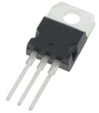
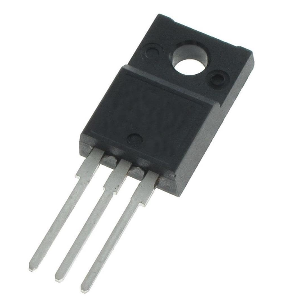
TK12A80W,S4X MOSFET Toshiba
地区:广东 深圳
认证:
无
图文详情
产品属性
相关推荐
TK12A80W,S4X
MOSFET N-Ch 800V 1400pF 23nC 11.5A 45W Silicon N-Channel MOS (DTMOS IV)
Applications TK12A80W,S4X
• Switching Voltage Regulators
Features TK12A80W,S4X
(1) Low drain-source on-resistance: RDS(ON) = 0.38 Ω (typ.) by using Super Junction Structure : DTMOS
(2) Easy to control Gate switching
(3) Enhancement mode: Vth = 3.0 to 4.0 V(VDS = 10 V, I D = 0.57 mA)
Absolute Maximum Ratings (Note) (T a = 25 unless otherwise specified) TK12A80W,S4X
Characteristics Drain-source voltage Gate-source voltage Drain current (DC) Drain current (pulsed) Power dissipation Single-pulse avalanche energy Single-pulse avalanche current Reverse drain current (DC) Reverse drain current (pulsed) Channel temperature Storage temperature Isolation voltage (RMS) Mounting torque (T c = 25 ) (t = 1.0 s) (Note 1) (Note 1) (Note 2) (Note 1) (Note 1) Symbol VDSS VGSS IDIDP PD EAS IAS IDR IDRP Tch Tstg VISO(RMS) TOR Rating 800 ±20 11.5 46 45 358 2.3 11.5 46 150 -55 to 150 2000 0.6 Unit VAW mJAV N m
Dynamic Characteristics (T a = 25 unless otherwise specified)
Characteristics Input capacitance Reverse transfer capacitance Output capacitance Effective output capacitance Gate resistance Switching time (rise time) Switching time (turn-on time) Switching time (fall time) Switching time (turn-off time) MOSFET dv/dt ruggedness Symbol Ciss Crss Coss Co(er) rgtr tontf toff dv/dt Test Condition VDS = 300 V, VGS = 0 V, f = 1 MHz VDS = 0 to 640 V, VGS = 0 V VDS = OPEN , f = 1 MHz See Figure 6.2.1 VDS ≤ V(BR)DSS, I D ≤ 11.5 A Min 50 Typ. 1400 3 29 35 30 40 70 11 130 Max Unit pFΩ ns V/ns


TK12A80W,S4X
TOSHIBA(东芝)
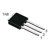
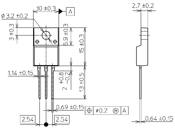
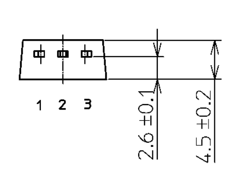
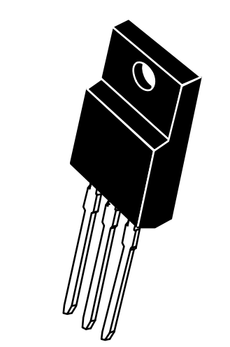
TO-220SIS-3
无铅环保型
直插式
单件包装
: 23 nC
: 800 V
: 11.5 A
: 380 mOhms