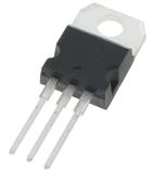

TK22E10N1,S1X MOSFET Toshiba
地区:广东 深圳
认证:
无
图文详情
产品属性
相关推荐
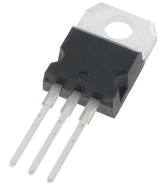
TK22E10N1,S1X
MOSFET N-Ch PWR FET 52A 72W 100V VDSS
Absolute Maximum Ratings (Note) (Ta = 25 unless otherwise specified) TK22E10N1,S1X
Characteristics Drain-source voltage Gate-source voltage Drain current (DC) Drain current (DC) Drain current (pulsed) Power dissipation Single-pulse avalanche energy Avalanche current Channel temperature Storage temperature (Tc = 25) (t = 1 ms) (Tc = 25) (Note 1) (Note 1,2) (Note 1) (Note 3) Symbol VDSS VGSS ID ID IDP PD EAS IAR Tch Tstg Rating 100 ±20 52 22 102 72 48 22 150 -55 to 150 Unit V A W mJ A
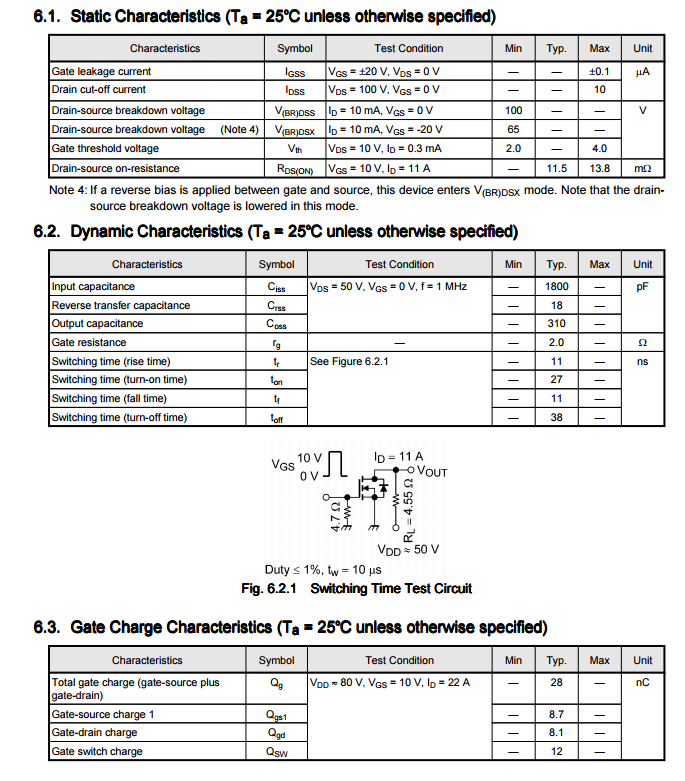
Dynamic Characteristics (Ta = 25 unless otherwise specified) TK22E10N1,S1X
Characteristics Input capacitance Reverse transfer capacitance Output capacitance Gate resistance Switching time (rise time) Switching time (turn-on time) Switching time (fall time) Switching time (turn-off time) Symbol Ciss Crss Coss rg tr ton tf toff Test Condition VDS = 50 V, VGS = 0 V, f = 1 MHz See Figure 6.2.1 Min Typ. 1800 18 310 2.0 11 27 11 38 Max Unit pF Ω ns
Static Characteristics (Ta = 25 unless otherwise specified) TK22E10N1,S1X
Characteristics Gate leakage current Drain cut-off current Drain-source breakdown voltage Drain-source breakdown voltage Gate threshold voltage Drain-source on-resistance (Note 4) Symbol IGSS IDSS V(BR)DSS V(BR)DSX Vth RDS(ON) Test Condition VGS = ±20 V, VDS = 0 V VDS = 100 V, VGS = 0 V ID = 10 mA, VGS = 0 V ID = 10 mA, VGS = -20 V VDS = 10 V, ID = 0.3 mA VGS = 10 V, ID = 11 A Min 100 65 2.0 Typ. 11.5 Max ±0.1 10 4.0 13.8 Unit μA V mΩ
TK22E10N1,S1X
TOSHIBA(东芝)
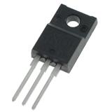
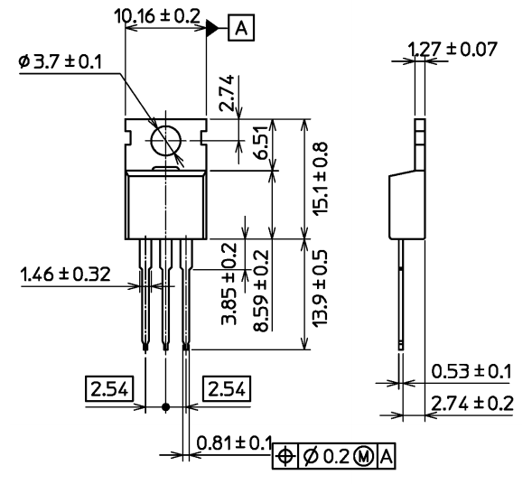
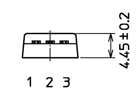
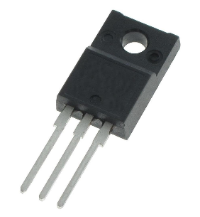
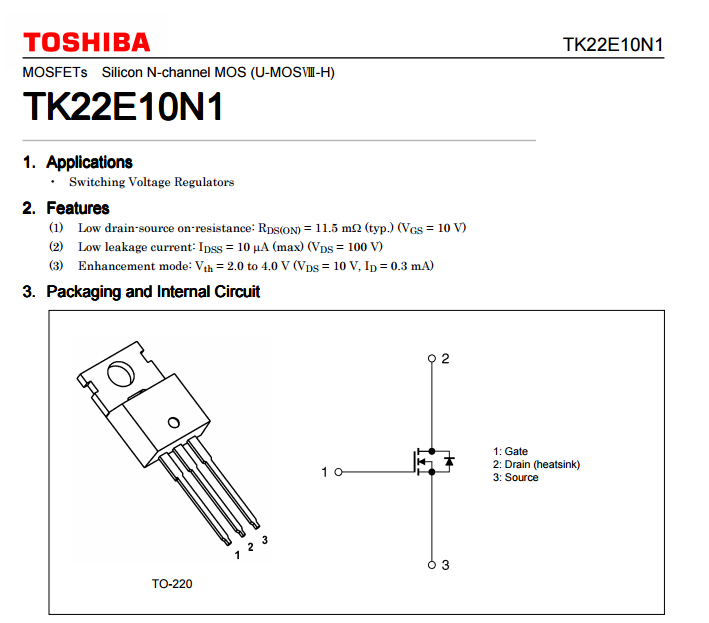
TO-220
无铅环保型
直插式
Through Hole
: 13.8 mOhms
: 100 V
: 6 g
: 52 A