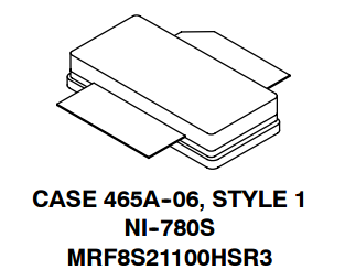
MRF8S21100HSR3 射频管 NXP
地区:广东 深圳
认证:
无
图文详情
产品属性
相关推荐
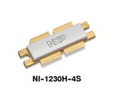
MRF8S21100HSR3
RF Power Field Effect Transistors
N--Channel Enhancement--Mode Lateral MOSFETs
射频金属氧化物半导体场效应(RF MOSFET)晶体管 HV8 2.1GHZ 100W
Designed for W--CDMA and LTE base station applications with frequencies
from 2110 to 2170 MHz. Can be used in Class AB and Class C for all typical
cellular base station modulation formats. MRF8S21100HSR3
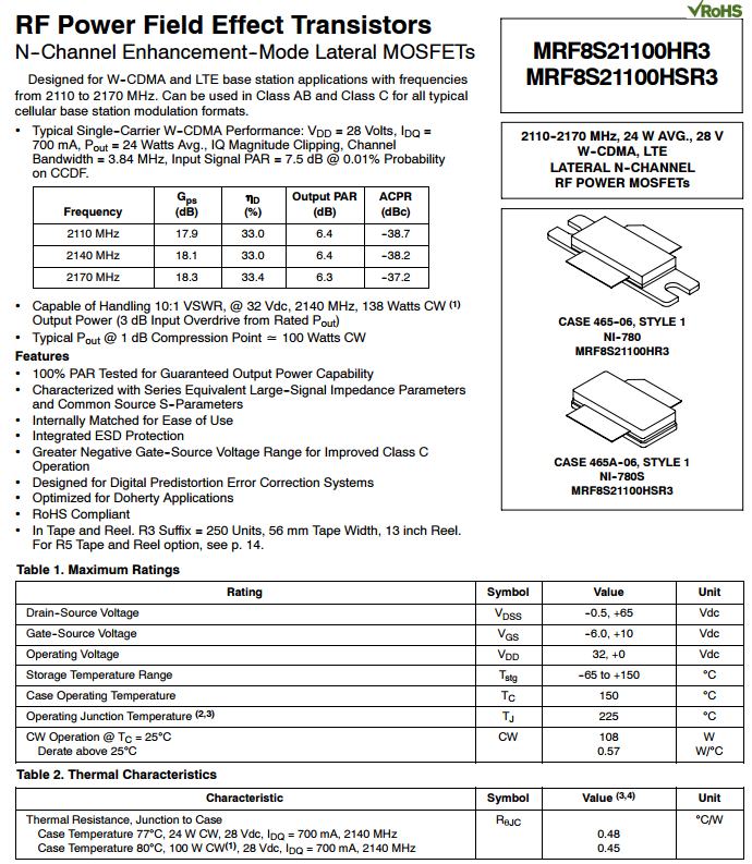
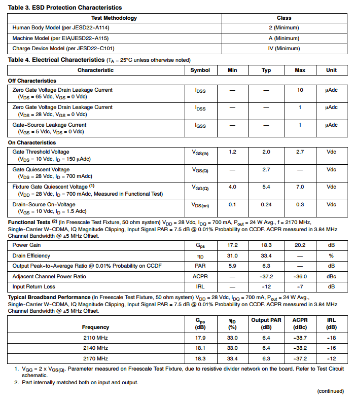
• Typical Single--Carrier W--CDMA Performance: VDD = 28 Volts, IDQ =
700 mA, Pout = 24 Watts Avg., IQ Magnitude Clipping, Channel
Bandwidth = 3.84 MHz, Input Signal PAR = 7.5 dB @ 0.01% Probability
on CCDF. MRF8S21100HSR3
Frequency
Gps
(dB)
ηD
(%)
Output PAR
(dB)
ACPR
(dBc)
2110 MHz 17.9 33.0 6.4 --38.7
2140 MHz 18.1 33.0 6.4 --38.2
2170 MHz 18.3 33.4 6.3 --37.2
• Capable of Handling 10:1 VSWR, @ 32 Vdc, 2140 MHz, 138 Watts CW (1)
Output Power (3 dB Input Overdrive from Rated Pout)
• Typical Pout @ 1 dB Compression Point ≃ 100 Watts CW
Features MRF8S21100HSR3
• 100% PAR Tested for Guaranteed Output Power Capability
• Characterized with Series Equivalent Large--Signal Impedance Parameters
and Common Source S--Parameters
• Internally Matched for Ease of Use
• Integrated ESD Protection
• Greater Negative Gate--Source Voltage Range for Improved Class C
Operation
• Designed for Digital Predistortion Error Correction Systems
• Optimized for Doherty Applications
• RoHS Compliant
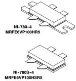
• In Tape and Reel. R3 Suffix = 250 Units, 56 mm Tape Width, 13 inch Reel.
For R5 Tape and Reel option, see p. 14.
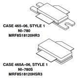
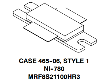
MRF8S21100HSR3
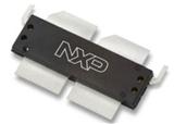
NXP(恩智浦)
NI-780S
无铅环保型
贴片式
单件包装
超大功率
超高频
NPN型
24 W
18.3 dB
65 V
N-Channel