在本系列的前几篇文章中,我们讨论了同步解调技术的基础知识。
在本文中,我们将了解用于实现基于方波的同步解调器的模拟块。我们还将简要介绍一下同步解调技术的 FPGA 实现。
基于方波的同步解调器
基于方波的同步解调器的框图如图 1 所示。
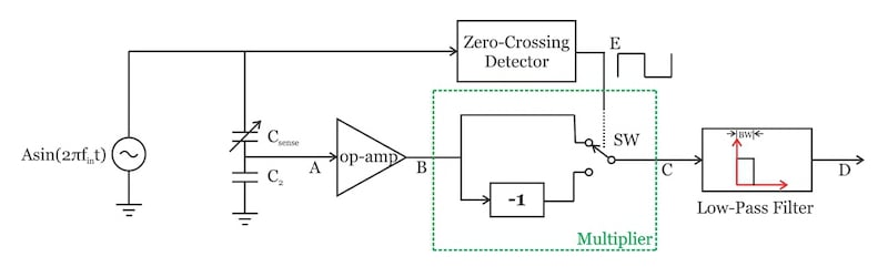
图 1. 基于方波的同步解调器
我们将检查的两个模块是“过零检测器”和“乘法器”。
过零检测器
“过零检测器”将输入正弦波转换为驱动开关 SW 的方波。这可以使用图 2 中的电路来完成。
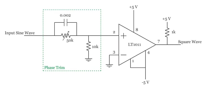
图 2.同步解调器中的过零检测器块。 原理图由 Linear Technology提供
LT1011是一个电压比较器,将输入正弦波与地电平进行比较。电位器用于调整产生的方波的相位,使其与图 1 中节点 B 处的正弦波相位相匹配。
这样,我们就可以得到一个方波,该方波在正弦波越过 0 V 时切换。回想一下,乘法器输出端的信号幅度是乘法器两个输入之间相位差的函数。当方波与正弦波同相时,两个信号之间的相位关系是已知的,我们可以更容易地解释出现在低通滤波器输出端的电压。
乘数
“乘法器”块的一种常见实现如图 3 所示:
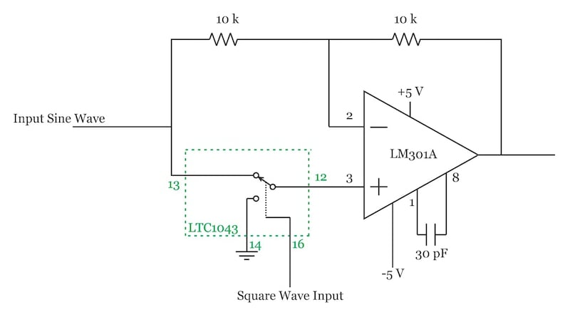
图 3. 示例同步解调器的乘法器块。原理图由 Linear Technology提供
在此图中,LM301A是一个通用运算放大器。LTC1043是一个构建块,初设计用于实现分立式开关电容器电路。图 4 显示了 LTC1043 内部部分电路的简化框图。
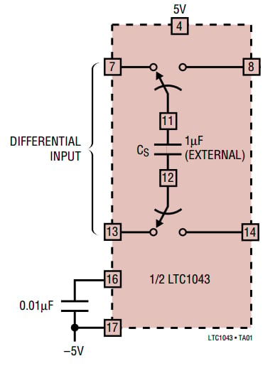
图 4. LTC1043 示意图。图片由凌力尔特提供
如图所示,差分输入在采样阶段连接到外部电容器。在下一阶段,充电的电容器连接到输出端口。可以在内部或通过外部 CMOS 时钟为开关创建时钟。
这个看似简单的功能使我们能够在各种应用中使用 LTC1043,例如精密仪表放大器和开关电容滤波器。然而,根据图 3 所示的原理图,LTC1043 实际上用作一个简单的开关。
让我们看看这个电路如何将输入乘以方波。当开关将端子 12 和 14 连接在一起时,我们有以下示意图。
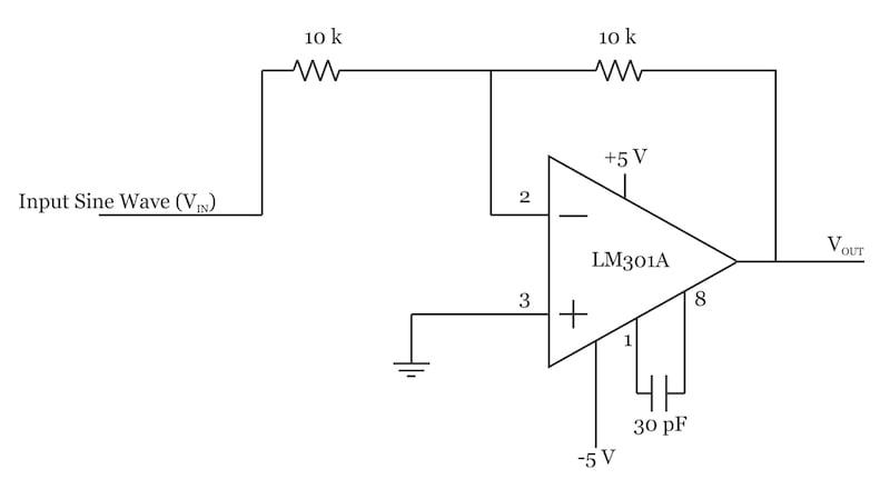
图 5
在这个操作阶段,我们有一个反相放大器,其增益为 VOUTVIN=?1。然而,当 LTC1043 的 12 和 13 端子连接在一起时,我们得到以下原理图:
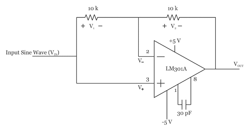
图 6. 连接 LTC1043 的端子 12 和 13
我们知道,由于负反馈通路和运算放大器的高增益,运算放大器的两个输入几乎具有相同的电压:V?=V+" role="presentation" style="box-sizing: inherit; border: 0px; display: inline-block; line-height: 0; font-size: 18.08px; word-wrap: normal; word-spacing: normal; white-space: nowrap; float: none; direction: ltr; max-width: none; max-height: none; min-width: 0px; min-height: 0px; margin: 0px; padding: 1px 0px; position: relative;">V?=V+。因此,V1=0V" role="presentation" style="box-sizing: inherit; border: 0px; display: inline-block; line-height: 0; font-size: 18.08px; word-wrap: normal; word-spacing: normal; white-space: nowrap; float: none; direction: ltr; max-width: none; max-height: none; min-width: 0px; min-height: 0px; margin: 0px; padding: 1px 0px; position: relative;">V1=0V 并且没有电流流过左侧的 10 kΩ 电阻。
假设运算放大器输入汲取的电流可以忽略不计,则通过反馈路径中 10 kΩ 电阻器的电流也将为零,我们有 V2=0V" role="presentation" style="box-sizing: inherit; border: 0px; display: inline-block; line-height: 0; font-size: 18.08px; word-wrap: normal; word-spacing: normal; white-space: nowrap; float: none; direction: ltr; max-width: none; max-height: none; min-width: 0px; min-height: 0px; margin: 0px; padding: 1px 0px; position: relative;">V2=0V。因此,在这个操作阶段,我们有 VOUTVIN=+1" role="presentation" style="box-sizing: inherit; border: 0px; display: inline-block; line-height: 0; font-size: 18.08px; word-wrap: normal; word-spacing: normal; white-space: nowrap; float: none; direction: ltr; max-width: none; max-height: none; min-width: 0px; min-height: 0px; margin: 0px; padding: 1px 0px; position: relative;">VOUTVIN=+1 的增益。换句话说,输入乘以在 ±1 之间切换的方波。
同步解调的数字实现
我们可以使用数字电路来实现同步解调器,而不是使用模拟构建块。基本思想如图 7 所示。
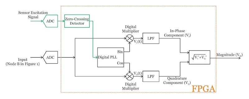
图 7.数字同步解调器电路
两个 A/D 转换器 (ADC) 用于将输入信号(图 1 中的节点 B)和传感器激励正弦波数字化。如图所示,其他块都是数字的,可以用FPGA实现。
同相和正交分量
在图 7 中,数字化输入与数字锁相环 (PLL) 产生的正弦波和余弦波相乘。为什么我们需要将输入乘以正弦波和余弦波?在本系列的部分中,我们研究了正弦波的乘法。如果我们将 vB(t)=Bsin(2πfint+?)" role="presentation" style="box-sizing: inherit; border: 0px; display: inline-block; line-height: 0; font-size: 18.08px; word-wrap: normal; word-spacing: normal; white-space: nowrap; float: none; direction: ltr; max-width: none; max-height: none; min-width: 0px; min-height: 0px; margin: 0px; padding: 1px 0px; position: relative;">vB(t)=Bsin(2πfint+?) 乘以 Asin(2πfint)" role="presentation" style="box-sizing: inherit; border: 0px; display: inline-block; line-height: 0; font-size: 18.08px; word-wrap: normal; word-spacing: normal; white-space: nowrap; float: none; direction: ltr; max-width: none; max-height: none; min-width: 0px; min-height: 0px; margin: 0px; padding: 1px 0px; position: relative;">Asin(2πfint),我们得到:
vC(t)=Asin(2πfint)×Bsin(2πfint+?)=12ABcos(?)?12ABcos(4πfint+?)" role="presentation" style="box-sizing: inherit; border: 0px; display: inline-block; line-height: 0; font-size: 18.08px; word-wrap: normal; word-spacing: normal; float: none; direction: ltr; max-width: none; max-height: none; min-width: 0px; min-height: 0px; margin: 0px; padding: 1px 0px; position: relative;">vC(t)=Asin(2πfint)×Bsin(2πfint+?)=12ABcos(?)?12ABcos(4πfint+?)
项是直流,但是,第二项是输入频率的两倍。因此,窄低通滤波器 (LPF) 可以去除第二项,我们有:
vI=12ABcos(?)" role="presentation" style="box-sizing: inherit; border: 0px; display: inline-block; line-height: 0; font-size: 18.08px; word-wrap: normal; word-spacing: normal; float: none; direction: ltr; max-width: none; max-height: none; min-width: 0px; min-height: 0px; margin: 0px; padding: 1px 0px; position: relative;">vI=12ABcos(?)
输出是两个输入之间相位差的函数。该等式表明,测量信号与参考输入之间的相位差会降低 LPF 输出端的信号幅度。
此外,我们需要知道相位差才能计算出被测信号的幅度。(请记住,上面讨论的模拟解决方案使用“相位微调”电路使相位差等于 0)。为了避免这两个问题,我们加入了第二个乘法阶段,将输入乘以余弦波:
vD(t)=Asin(2πfint)×Bsin(2πfint+?)=12ABsin(?)+12ABsin(4πfint+?)" role="presentation" style="box-sizing: inherit; border: 0px; display: inline-block; line-height: 0; font-size: 18.08px; word-wrap: normal; word-spacing: normal; float: none; direction: ltr; max-width: none; max-height: none; min-width: 0px; min-height: 0px; margin: 0px; padding: 1px 0px; position: relative;">vD(t)=Asin(2πfint)×Bsin(2πfint+?)=12ABsin(?)+12ABsin(4πfint+?)
在 LPF 之后,我们有:
vQ=12ABsin(?)" role="presentation" style="box-sizing: inherit; border: 0px; display: inline-block; line-height: 0; font-size: 18.08px; word-wrap: normal; word-spacing: normal; float: none; direction: ltr; max-width: none; max-height: none; min-width: 0px; min-height: 0px; margin: 0px; padding: 1px 0px; position: relative;">vQ=12ABsin(?)
我们可以通过对同相和正交分量的平方和求平方根来计算输入的幅度:
vM=vI2+vQ2=12AB" role="presentation" style="box-sizing: inherit; border: 0px; display: inline-block; line-height: 0; font-size: 18.08px; word-wrap: normal; word-spacing: normal; float: none; direction: ltr; max-width: none; max-height: none; min-width: 0px; min-height: 0px; margin: 0px; padding: 1px 0px; position: relative;">vM=√vI2+vQ2=12AB
如您所见,结果不是相位差的函数。
数字锁相环
请务必注意,图 7 中的数字 PLL 必须生成正弦和余弦波形样本。我们可以通过使用具有直接数字合成器 (DDS)作为其数字控制振荡器 (DCO) 的PLL 来实现这一点。基本思想如图 8 所示。
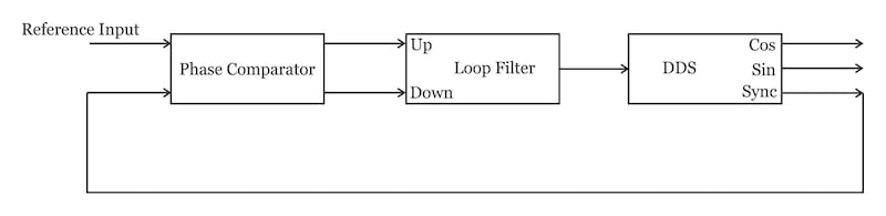
图 8.带有直接数字合成器的 PLL。图片改编自康奈尔大学
您可以在此处找到有关同步解调器的 FPGA 实现的更多信息。
结论
在本文中,我们检查了同步解调技术的模拟和数字实现:
对于模拟实现,我们需要一个“过零检测器”和一个“乘法器”。
对于数字版本,我们可以使用两个 ADC 将测量信号和传感器激励波形数字化。
其他块可以在 FPGA 中实现。通过实施同相和正交路径,我们可以使测量独立于乘法器输入之间的相位差。对于数字实现,我们需要一个 PLL 来生成正弦和余弦波形样本。这可以通过使用 DDS 作为可编程振荡器的 PLL 来实现。