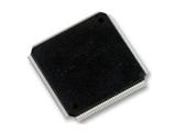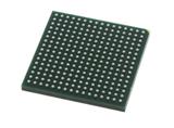
LFE3-35EA-6FN484C FPGA
地区:广东 深圳
认证:
无
图文详情
产品属性
相关推荐
LFE3-35EA-6FN484C
FPGA - 现场可编程门阵列 33.3K LUTs 295 I/O 1.2V -6 Speed
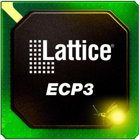
Introduction
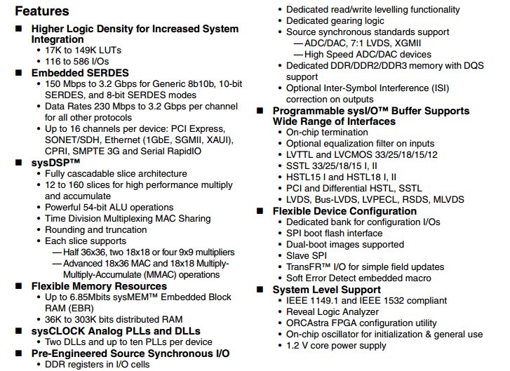
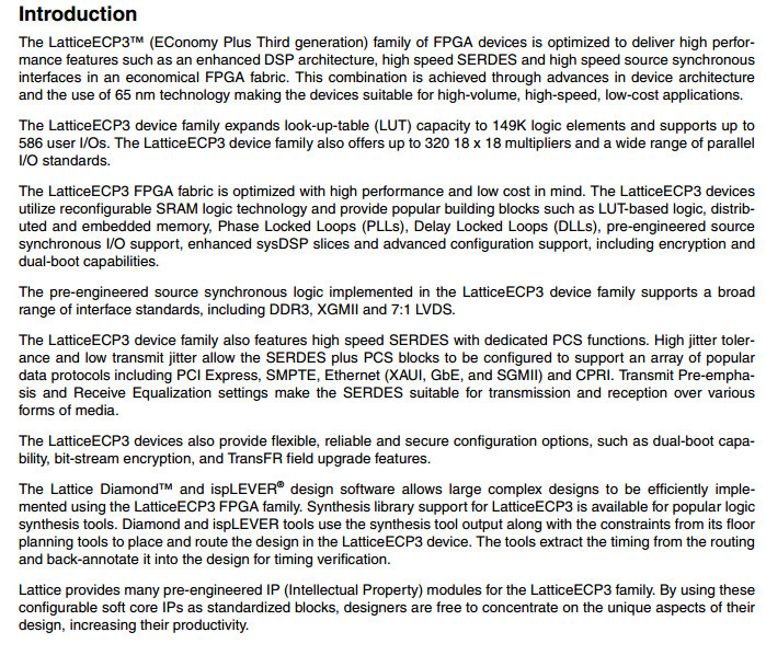
The LFE3-35EA-6FN484C LatticeECP3™ (EConomy Plus Third generation) family of FPGA devices is optimized to deliver high performance features such as an enhanced DSP architecture, high speed SERDES and high speed source synchronous interfaces in an economical FPGA fabric. This combination is achieved through advances in device architecture and the use of 65 nm technology making the devices suitable for high-volume, high-speed, low-cost applications.
The LFE3-35EA-6FN484C LatticeECP3 device family expands look-up-table (LUT) capacity to 149K logic elements and supports up to 586 user I/Os. The LatticeECP3 device family also offers up to 320 18 x 18 multipliers and a wide range of parallel I/O standards.
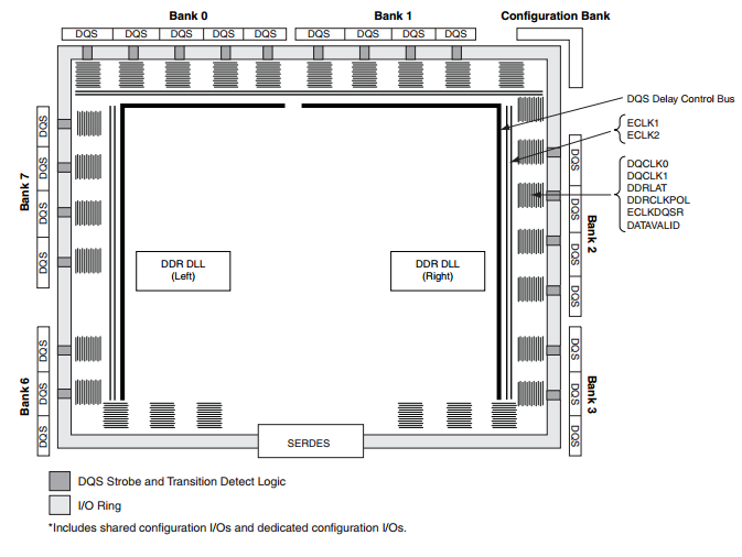
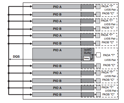
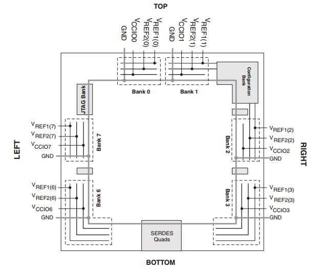
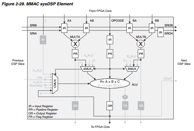
The LFE3-35EA-6FN484C LatticeECP3 FPGA fabric is optimized with high performance and low cost in mind. The LatticeECP3 devices utilize reconfigurable SRAM logic technology and provide popular building blocks such as LUT-based logic, distributed and embedded memory, Phase Locked Loops (PLLs), Delay Locked Loops (DLLs), pre-engineered source synchronous I/O support, enhanced sysDSP slices and advanced configuration support, including encryption and dual-boot capabilities.
: 1327 kbit
: 68 kbit
: 89.3 mA
: 1.2 V
: - 40 ℃
: + 100 ℃