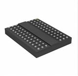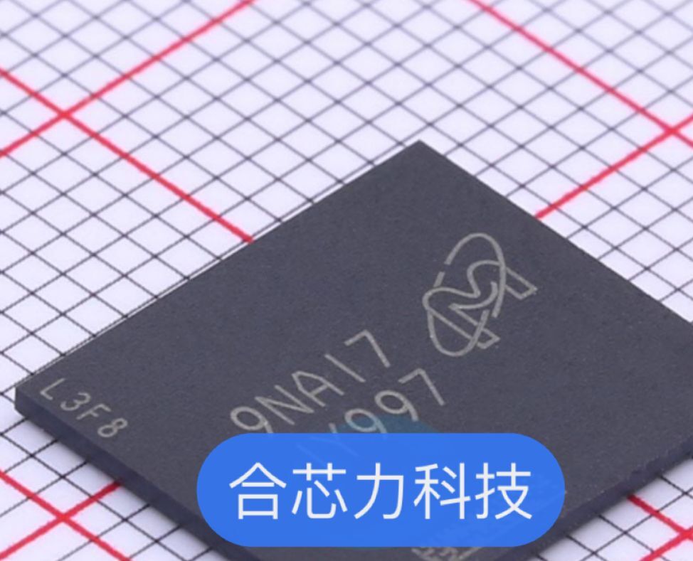


SDRAM存储器MT47H64M16NF-25E IT:M
地区:广东 深圳
认证:
无
图文详情
产品属性
相关推荐
MT47H64M16NF-25E IT:M MT47H64M16NF-25E IT:M MT47H64M16NF-25E IT:M
MT47H64M16NF-25E IT:M
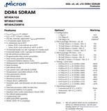
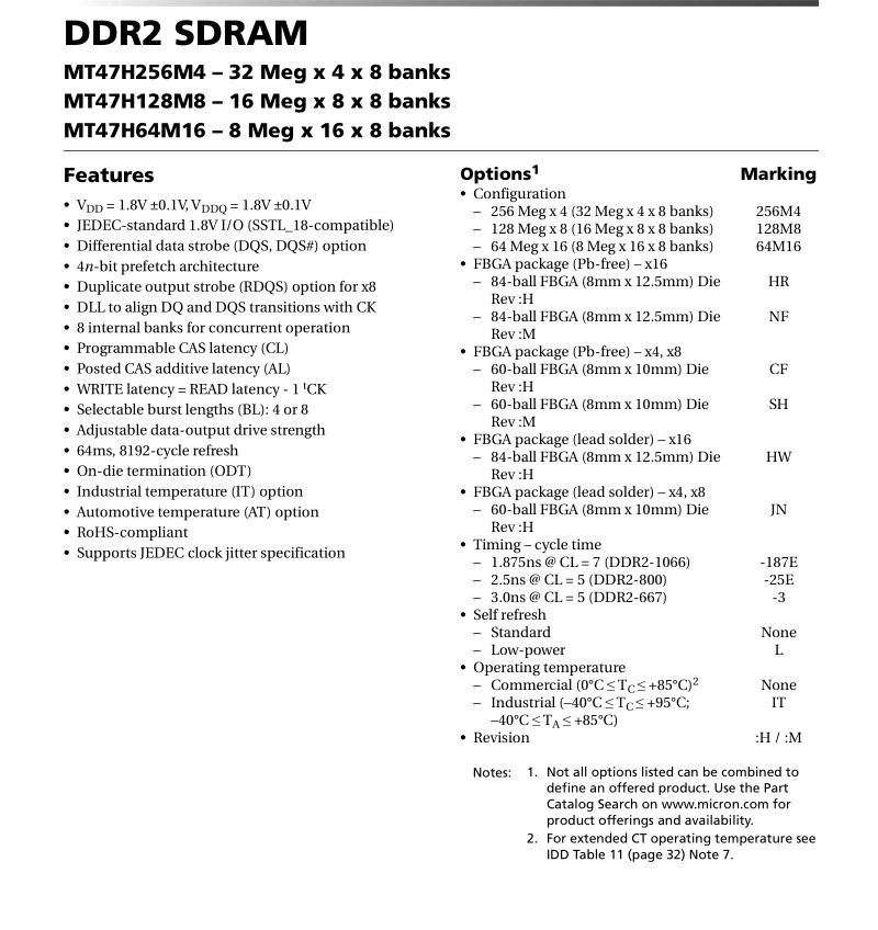
Features
• V DD = 1.8V ±0.1V, V DDQ = 1.8V ±0.1V
• JEDEC-standard 1.8V I/O (SSTL_18-compatible)
• Differential data strobe (DQS, DQS#) option
• 4n-bit prefetch architecture
• Duplicate output strobe (RDQS) option for x8
• DLL to align DQ and DQS transitions with CK
• 8 internal banks for concurrent operation
• Programmable CAS latency (CL)
• Posted CAS additive latency (AL)
• WRITE latency = READ latency - 1 t CK
• Selectable burst lengths (BL): 4 or 8
• Adjustable data-output drive strength
• 64ms, 8192-cycle refresh
• On-die termination (ODT)
• Industrial temperature (IT) option
• Automotive temperature (AT) option
• RoHS-compliant
• Supports JEDEC clock jitter specification
Options 1 Marking
• Configuration
– 256 Meg x 4 (32 Meg x 4 x 8 banks) 256M4
– 128 Meg x 8 (16 Meg x 8 x 8 banks) 128M8
– 64 Meg x 16 (8 Meg x 16 x 8 banks) 64M16
• FBGA package (Pb-free) – x16
– 84-ball FBGA (8mm x 12.5mm) Die
Rev :H
HR
– 84-ball FBGA (8mm x 12.5mm) Die
Rev :M
NF
• FBGA package (Pb-free) – x4, x8
– 60-ball FBGA (8mm x 10mm) Die
Rev :H
CF
– 60-ball FBGA (8mm x 10mm) Die
Rev :M
SH
• FBGA package (lead solder) – x16
– 84-ball FBGA (8mm x 12.5mm) Die
Rev :H
HW
• FBGA package (lead solder) – x4, x8
– 60-ball FBGA (8mm x 10mm) Die
Rev :H
JN
• Timing – cycle time
– 1.875ns @ CL = 7 (DDR2-1066) -187E
– 2.5ns @ CL = 5 (DDR2-800) -25E
– 3.0ns @ CL = 5 (DDR2-667) -3
• Self refresh
– Standard None
– Low-power L
• Operating temperature
– Commercial (0°C ? T C ? +85°C) 2 None
– Industrial (–40°C ? T C ? +95°C;
–40°C ? T A ? +85°C)
IT
• Revision :H / :M


SDRAM存储器
FBGA-84
64 Meg x 16
1.8V ±0.1V
–40°C~+95°C
SDRAM存储器MT41K256M8DA-125:K
SDRAM存储器MT41K256M16HA-125:E
DDR4-4G存储器MT40A256M16GE-083E:B
SDRAM存储器MT48LC16M16A2P-6A
供应MT41K256M16TW-107 AAT:P BGA-96
供应W631GG6MB-11 FBGA96 WINBOND
Micron MT53E128M32D2DS-053 AUT:A SDRAM
NT5CB256M16CP-FL 优势供应NANYA原装DDR3
H5TQ4G83AFR-PBC SKhynix原装DDR3 现货供应
H5GC4H24AJR-R0C 海力士原装GDDR5 库存现货