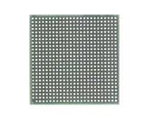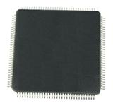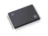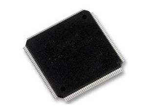


LCMXO640C-3TN144C FPGA
地区:广东 深圳
认证:
无
图文详情
产品属性
相关推荐
LCMXO640C-3TN144C
FPGA - 现场可编程门阵列 640 LUTS 113 I/O
Introduction LCMXO640C-3TN144C
The MachXO is optimized to meet the requirements of
applications traditionally addressed by CPLDs and low
capacity FPGAs: glue logic, bus bridging, bus interfacing,
power-up control, and control logic. These devices
bring together the best features of CPLD and FPGA
devices on a single chip.
Features LCMXO640C-3TN144C
Non-volatile, Infinitely Reconfigurable
• Instant-on – powers up in microseconds
• Single chip, no external configuration memory required
• Excellent design security, no bit stream to intercept
• Reconfigure SRAM based logic in milliseconds
• SRAM and non-volatile memory programmable
through JTAG port
• Supports background programming of
non-volatile memory LCMXO640C-3TN144C
TransFR™ Reconfiguration (TFR)
• In-field logic update while system operates
High I/O to Logic Density
• 256 to 2280 LUT4s
• 73 to 271 I/Os with extensive package options
• Density migration supported
• Lead free/RoHS compliant packaging
Embedded and Distributed Memory
• Up to 27.6 Kbits sysMEM™ Embedded Block RAM
• Up to 7.7 Kbits distributed RAM
• Dedicated FIFO control logic
Flexible I/O Buffer
• Programmable sysIO™ buffer supports wide
range of interfaces:
— LVCMOS 3.3/2.5/1.8/1.5/1.2
— LVTTL
— PCI
— LVDS, Bus-LVDS, LVPECL, RSDS
sysCLOCK™ PLLs
• Up to two analog PLLs per device
• Clock multiply, divide, and phase shifting
System Level Support
• IEEE Standard 1149.1 Boundary Scan
• Onboard oscillator
• Devices operate with 3.3 V, 2.5 V, 1.8 V or 1.2 V
power supply
• IEEE 1532 compliant in-system programming


: 113 I/O
: 1.8 V, 2.5 V, 3.3 V
: 17 mA
: 6.1 kbit
: 0 ℃
: + 85 ℃