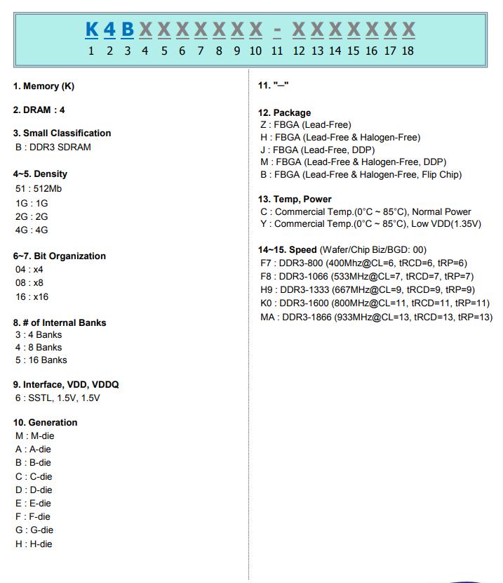


供应K4B4G1646D-BFMA 原装 DDR3
地区:广东 深圳
认证:
无
图文详情
产品属性
相关推荐
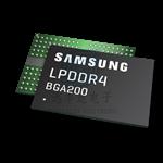
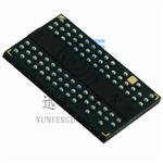
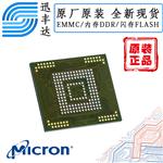
K4B4G1646D-BFMA 原装 DDR3
K4B4G1646D-BFMA03V
DDR3 SDRAM Specification
K4B4G1646D-BFMA 原装 DDR3 的技术参数:
|
型号 |
K4B4G1646D-BFMA |
|
制造商 |
SAMSUNG |
|
RoHS |
是 |
|
类别 |
集成电路(IC) 存储器 |
|
封装 / 箱体 |
FBGA-96 |
|
容量 |
4 Gb |
|
组织 |
256M x 16 |
|
速率 |
1866 Mbps |
|
工作电压 |
1.35V |
|
温度规格 |
-40 ~ 95 °C |
|
产品类型 |
DRAM DDR3 |
K4B4G1646D-BFMA 原装 DDR3 的描述
The DDR3 SDRAM is a high-speed CMOS, dynamic random-access memory internally configured as a eight-bank DRAM. The DDR3 SDRAM uses a 8n prefetch architecture to achieve high-speed operation. The 8n prefetch architecture, with an interface designed to transfer two data words per clock cycle at the I/O pins.
A single read or write access for the DDR3 SDRAM consists of a single 8n-bit wide, four clock data transfer at the internal DRAM core and two corresponding n-bit wide, one-half clock cycle data transfers at the I/O pins.
Read and write operation to the DDR3 SDRAM are burst oriented, start at a selected location, and continue for a burst length of four or eight in a programmed sequence. Operation begins with the registration of an Active command, which is then followed by a Read or Write command. The address bits registered coincident with the Active command are used to select the bank and row to be accessed (BA0-BA2 select the bank; A0-A15 select the row).
The address bits registered coincident with the Read or Write command are used to select the starting column location for the burst operation, determine if the auto precharge command is to be issued (via A10/AP), and the select BC4 or BL8 mode ’on the fly’ (via A12) if enabled in the mode register. Prior to normal operation, the DDR3 SDRAM must be powered up and initialized in a predefined manner. The following sections provide detailed information covering device reset and initialization, register definition, command descriptions and device operation.


K4B4G1646D-BFMA
SAMSUNG/三星
FBGA
22+
无铅/环保