
原装MT41K256M16HA-125:E LPDDR3供应
地区:广东 深圳
认证:
无
图文详情
产品属性
相关推荐
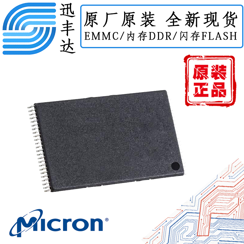
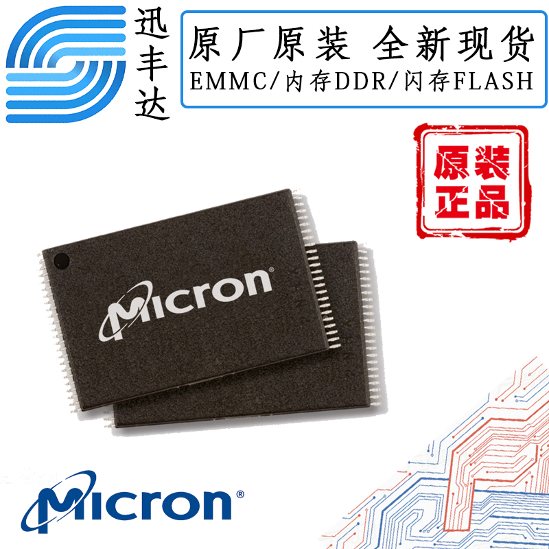
原装MT41K256M16HA-125:E LPDDR3
IC DRAM 4GBIT PARALLEL 96FBGA
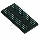
SDRAM - DDR3L 存储器 IC 4Gb(256M x 16) 并联 800 MHz 13.75 ns 96-FBGA(9x14)
原装MT41K256M16HA-125:E LPDDR3的技术参数:
类别 存储器
制造商 Micron Technology Inc.
存储器类型 易失
存储器格式 DRAM
技术 SDRAM - DDR3L
存储容量 4Gb(256M x 16)
存储器接口 并联
时钟频率 800 MHz
电压 - 供电 1.283V ~ 1.45V
工作温度 0°C ~ 95°C(TC)
安装类型 表面贴装型
封装/外壳 96-TFBGA
供应商器件封装 96-FBGA(9x14)
RoHS 状态 符合 ROHS3 规范
湿气敏感性等级 (MSL) 3(168 小时)
REACH 状态 非 REACH 产品
ECCN EAR99
HTSUS 8542.32.0036
原装MT41K256M16HA-125:E LPDDR3的描述:
DDR3L SDRAM (1.35V) is a low voltage version of the DDR3 (1.5V) SDRAM.
DDR3 SDRAM uses a double data rate architecture to achieve high-speed operation.
The double data rate architecture is an 8n-prefetch architecture with an interface designed to transfer two data words per clock cycle at the I/O pins.
A single read or write operation for the DDR3 SDRAM effectively consists of a single 8n-bit-wide, four-clockcycle data transfer at the internal DRAM core and eight corresponding n-bit-wide, onehalf-clock-cycle data transfers at the I/O pins.
The differential data strobe (DQS, DQS#) is transmitted externally, along with data, for use in data capture at the DDR3 SDRAM input receiver. DQS is center-aligned with data for WRITEs.
The read data is transmitted by the DDR3 SDRAM and edge-aligned to the data strobes.
The DDR3 SDRAM operates from a differential clock (CK and CK#).
The crossing of CK going HIGH and CK# going LOW is referred to as the positive edge of CK. Control, command, and address signals are registered at every positive edge of CK. Input data is registered on the first rising edge of DQS after the WRITE preamble, and output data is referenced on the first rising edge of DQS after the READ preamble.
Read and write accesses to the DDR3 SDRAM are burst-oriented. Accesses start at a selected location and continue for a programmed number of locations in a programmed
sequence. Accesses begin with the registration of an ACTIVATE command, which is then
followed by a READ or WRITE command. The address bits registered coincident with
the ACTIVATE command are used to select the bank and row to be accessed. The address bits registered coincident with the READ or WRITE commands are used to select
the bank and the starting column location for the burst access.
The device uses a READ and WRITE BL8 and BC4. An auto precharge function may be
enabled to provide a self-timed row precharge that is initiated at the end of the burst
access.
As with standard DDR SDRAM, the pipelined, multibank architecture of DDR3 SDRAM
allows for concurrent operation, thereby providing high bandwidth by hiding row precharge and activation time.
A self refresh mode is provided, along with a power-saving, power-down mode.


MT41K256M16HA-125:E
MICRON/镁光
BGA
21+/22+
96