

原装MT41K128M16JT-125IT:K LPDDR3供应
地区:广东 深圳
认证:
无
图文详情
产品属性
相关推荐
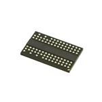
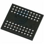
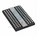
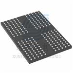
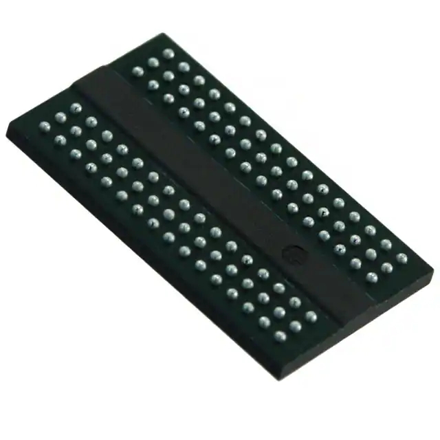
MT41K128M16JT-125IT:K LPDDR3
IC DRAM 2GBIT PARALLEL 96FBGA
动态随机存取存储器 LPDDR3 2G 128MX16 FBGA
SDRAM - DDR3L 存储器 IC 2Gb(128M x 16) 并联 800 MHz 13.75 ns 96-FBGA(8x14)
MT41K128M16JT-125IT:K LPDDR3的技术参数:
类别 : 存储器
缩写 : D9PSK
制造商 : Micron Technology Inc.
存储器类型 : 易失
存储器格式 : DRAM
技术 : SDRAM - DDR3L
存储容量 : 2Gb(128M x 16)
存储器接口 : 并联
时钟频率 : 800 MHz :
电压 - 供电 : 1.283V ~ 1.45V
工作温度 : -40°C ~ 95°C(TC)
安装类型 : 表面贴装型
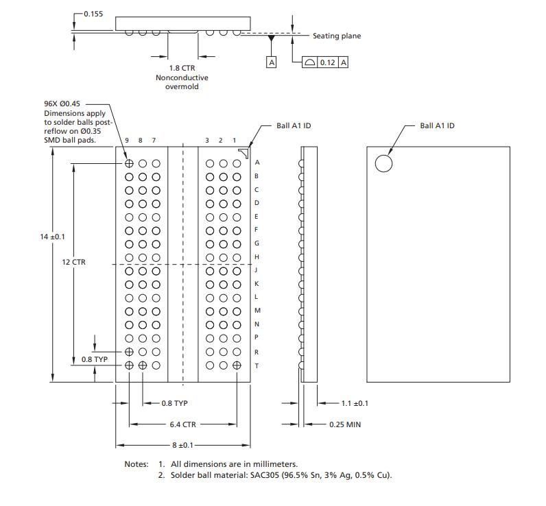
封装/外壳 : 96-TFBGA
供应商器件封装 : 96-FBGA(8x14)
基本产品编号 : MT41K128M16
RoHS 状态 : 符合 ROHS3 规范
湿气敏感性等级 (MSL) : 3(168 小时)
REACH 状态 : 非 REACH 产品
ECCN : EAR99
HTSUS : 8542.32.0036
速度:800MHz
接口:并联
电压 - 电源:1.283 V ~ 1.45 V
描述:
DDR3 SDRAM uses a double data rate architecture to achieve high-speed operation.
The double data rate architecture is an 8n-prefetch architecture with an interface designed to transfer two data words per clock cycle at the I/O pins.
A single read or write operation for the DDR3 SDRAM effectively consists of a single 8n-bit-wide, four-clockcycle data transfer at the internal DRAM core and eight corresponding n-bit-wide, onehalf-clock-cycle data transfers at the I/O pins.
The differential data strobe (DQS, DQS#) is transmitted externally, along with data, for use in data capture at the DDR3 SDRAM input receiver.
DQS is center-aligned with data for WRITEs.
The read data is transmitted by the DDR3 SDRAM and edge-aligned to the data strobes.
The DDR3 SDRAM operates from a differential clock (CK and CK#).
The crossing of CK going HIGH and CK# going LOW is referred to as the positive edge of CK.
Control, command, and address signals are registered at every positive edge of CK. Input data is registered on the first rising edge of DQS after the WRITE preamble, and output data is referenced on the first rising edge of DQS after the READ preamble.

MT41K128M16JT-125IT:K
MICRON/镁光
FBGA
21+/22+
96