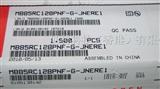
供应富士通铁电存储器 *85RS64APNF-G-JNERE1
地区:广东 深圳
认证:
无
图文详情
产品属性
相关推荐
原厂原装无铅现货,11+,可替代*5CL6*-GTR,和*5CL6*-GATR
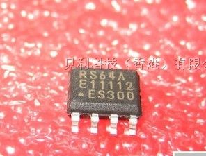
The *85RS64APNF-G-JNERE1 is a FRAM (Ferroelectric Random Access Memory) chip in a configuration of 8,192 words × 8bits, using the ferroelectric process and silicon gate CMOS process technologies for forming the nonvolatile memory cells. The *85RS64APNF-G-JNERE1 adopts the Serial Peripheral Interface (SPI). The device is able to retain data without using a back-up battery, as is needed for SRAM. The memory cells used in the *85RS64APNF-G-JNERE1 can be used for 1010 read/write operations, which is a significant improvement over the number of read and write operations supported by Flash memory and E2PROM. The *85RS64APNF-G-JNERE1 does not take long time to write data unlike Flash memories nor E2PROM.
*85RS64APNF-G-JNERE1 absolute maximum ratings: (1)Power supply voltage, VCC: -0.5 to 4.0V; (2)Input voltage, VIN: -0.5 to VCC+0.5V; (3)Output voltage, VOUT: -0.5 to VCC+0.5V; (4)Operating temperature, TA: -40 to 85℃; (5)Storage temperature, Tstg: -40 to 125℃.
*85RS64APNF-G-JNERE1 features: (1)Bit configuration: 8,192 words×8 bits; (2)Operating power supply voltage: 3.0 to 3.6V; (3)Operating frequency: 20MHz (Max); (4)Serial Peripheral Interface: SPI (Serial Peripheral Interface); Correspondent to SPI mode 0 (0, 0) and mode 3 (1, 1); (5)Operating temperature range: -40 to +85℃; (6)Data retention: 10 years (+55℃); (7)High endurance: 10 Billion Read/writes; (8)Package: 8-pin plastic SOP (FPT-8P-M02).
*85RS64APNF-G-JNERE1
FUJITSU