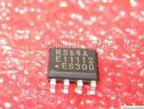
供应富士通铁电存储器 *85RC128PNF-G-JNERE1
地区:广东 深圳
认证:
无
图文详情
产品属性
相关推荐
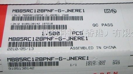
*原厂原装无铅现货,10+,1500/盘
The *85RC128PNF-G-JNERE1 is a FRAM (Ferroelectric Random Access Memory) Stand-Alone chip in a configuration of 16,384 words * 8 bits, using the ferroelectric process and silicon gate CMOS process technologies for forming the nonvolatile memory cells. The *85RC128PNF-G-JNERE1 adopts the two-wire serial interface. Unlike SRAM, the device is able to retain data without using a data backup battery. The read/write endurance of the nonvolatile memory cells used for the *85RC128PNF-G-JNERE1 has improved to be at least 1010 cycles, significantly out performing Flash memory and E2PROM in the number. The device does not need a polling sequence after writing to the memory such as the case of Flash memory nor E2PROM.
*85RC128PNF-G-JNERE1 absolute maximum ratings: (1)Power supply voltage:-0.5V to +4.0 V; (2)Input pin voltage:-0.5V to VCC + 0.5 ( ≤ 4.0) V; (3)Output pin voltage:-0.5V to VCC + 0.5 ( ≤ 4.0) V; (4)Ambient temperature:-40℃ to + 85℃; (5)Storage temperature:-40℃ to + 125℃.
*85RC128PNF-G-JNERE1 features: (1)Bit configuration :16,384 words * 8 bits ; (2)Operating power supply voltage : 2.7 V to 3.6 V; (3)Operating frequency : 400 kHz (Max) ; (4)Two-wire serial interface : I2C-bus specification ver. 2.1 compliant, supports Standard-mode/Fast-mode.Fully controllable by two ports: serial clock (SCL) and serial data(SDA); (5)Operating temperature range:-40℃ to +85℃; (6)Data retention : 10 years ( + 75℃) ; (7)Read/write endurance : 1010 times; (8)Package : Plastic / SOP, 8-pin (FPT-8P-M02); (9)Low power consumption : Operating current 0.15 mA (Max: @400 kHz), Standby current 5 μA (T*).
*85RC128PNF-G-JNERE1
FUJITSU