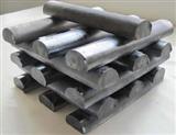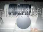
氮化镓GaN氮化镓GaN wafer 北京特博万德科技
地区:北京 北京市
认证:
无
图文详情
产品属性
相关推荐
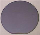
Specifications:
|
Item |
GaN-FS-N |
|
Dimensions |
Ф50.8mm±1mm |
|
Thickness |
300 ± 25 μm |
|
Orientation |
C-axis(0001) ± 0.5° |
|
Orientation Flat |
(1-100) ± 0.5°, 16.0 ±1.0mm |
|
Secondary Orientation Flat |
(11-20) ± 3°, 8.0 ±1.0mm |
|
TTV |
≤15 μm |
|
BOW |
≤20 μm |
|
Conduction Type |
N-type |
|
Resistivity(300K) |
< 0.5 Ω·cm |
|
Dislocation Density |
Less than 5x106 cm-2 |
|
Useable Surface Area |
> 90% |
|
Polishing |
Front Surface: Ra < 0.2nm. Epi-ready polished Back Surface: Fine ground |
|
Package |
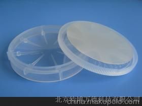
Packaged in a class 100 clean room environment, in single wafer containers, under a nitrogen atmosphere. |
|
Item |
GaN-FS-10 |
|
Dimensions |
10.0mm×10.5mm |
|
Thickness |
300 ± 25 μm |
|
Orientation |
C-axis(0001) ± 0.5° |
|
TTV |
≤15 μm |
|
BOW |
≤20 μm |
|
Conduction Type |
N-type |
|
Resistivity(300K) |
< 0.5 Ω·cm |
|
Dislocation Density |
Less than 5x106 cm-2 |
|
Useable Surface Area |
> 90% |
|
Polishing |
Front Surface: Ra < 0.2nm. Epi-ready polished Back Surface: Fine ground |
可选择
北京