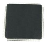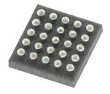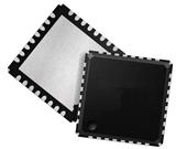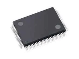
LCMXO256C-3TN100C FPGA
地区:广东 深圳
认证:
无
图文详情
产品属性
相关推荐
LCMXO256C-3TN100C
FPGA - 现场可编程门阵列 256 LUTS 78 I/O
Introduction LCMXO256C-3TN100C
The MachXO is optimized to meet the requirements of applications traditionally addressed by CPLDs and low capacity FPGAs: glue logic, bus bridging, bus interfacing, power-up control, and control logic. These devices bring together the best features of CPLD and FPGA devices on a single chip.
Architecture Overview LCMXO256C-3TN100C
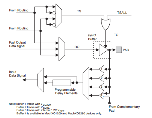
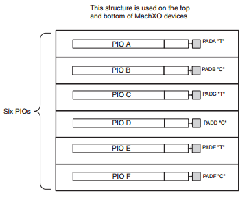
The MachXO family architecture contains an array of logic blocks surrounded by Programmable I/O (PIO). Some devices in this family have sysCLOCK PLLs and blocks of sysMEM™ Embedded Block RAM (EBRs). Figures 2-1, 2-2, and 2-3 show the block diagrams of the various family members.
Features LCMXO256C-3TN100C
Non-volatile, Infinitely Reconfigurable
• Instant-on – powers up in microseconds
• Single chip, no external configuration memory
required
• Excellent design security, no bit stream to
intercept
• Reconfigure SRAM based logic in milliseconds
• SRAM and non-volatile memory programmable
through JTAG port
• Supports background programming of
non-volatile memory
Sleep Mode
• Allows up to 100x static current reduction
TransFR™ Reconfiguration (TFR)
• In-field logic update while system operates
High I/O to Logic Density
• 256 to 2280 LUT4s
• 73 to 271 I/Os with extensive package options
• Density migration supported
• Lead free/RoHS compliant packaging
: 13 mA
: 1.8 V, 2.5 V, 3.3 V
: 0 ℃
: + 85 ℃
: 2 kbit
: 78 I/O