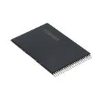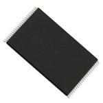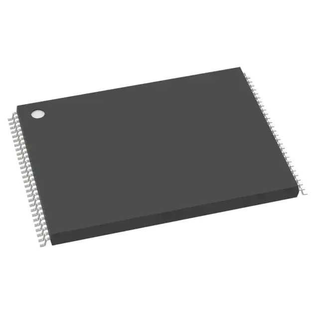
原装MT29F4G08ABAEAWP:E NAND FLASH
地区:广东 深圳
认证:
无
图文详情
产品属性
相关推荐
原装MT29F4G08ABAEAWP:E NAND FLASH
MT29F4G08ABAEAWP:E(托盘)
MT29F4G08ABAEAWP:E TR(卷带:1000)
IC FLASH 4GBIT PARALLEL 48TSOP I
闪存 - NAND 存储器 IC 4Gb(512M x 8) 并联 48-TSOP I
原装MT29F4G08ABAEAWP:E NAND FLASH的技术参数:
存储器类型 非易失
存储器格式 闪存
技术 闪存 - NAND
存储容量 4Gb(512M x 8)
存储器接口 并联
电压 - 供电 2.7V ~ 3.6V
工作温度 0°C ~ 70°C(TA)
安装类型 表面贴装型
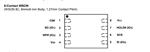
封装/外壳 48-TFSOP(0.724",18.40mm 宽)
供应商器件封装 48-TSOP I
基本产品编号 MT29F4G08
RoHS 状态 符合 ROHS3 规范
湿气敏感性等级 (MSL) 3(168 小时)
REACH 状态 非 REACH 产品
ECCN 3A991B1A
HTSUS 8542.32.0071
一般说明
Micron NAND Flash devices include an asynchronous data interface for high-performance I/O operations. These devices use a highly multiplexed 8-bit bus (I/Ox) to transfer commands, address, and data. There are five control signals used to implement the asynchronous data interface: CE#, CLE, ALE, WE#, and RE#. Additional signals control hardware write protection and monitor device status (R/B#).
This hardware interface creates a low pin-count device with a standard pinout that remains the same from one density to another, enabling future upgrades to higher densities with no board redesign.
A target is the unit of memory accessed by a chip enable signal. A target contains one or
more NAND Flash die. A NAND Flash die is the minimum unit that can independently
execute commands and report status. A NAND Flash die, in the ONFI specification, is
referred to as a logical unit (LUN). There is at least one NAND Flash die per chip enable
signal. For further details, see Device and Array Organization.
This device has an internal 4-bit ECC that can be enabled using the GET/SET features
or by factory (always enabled). See Internal ECC and Spare Area Mapping for ECC for
more information.

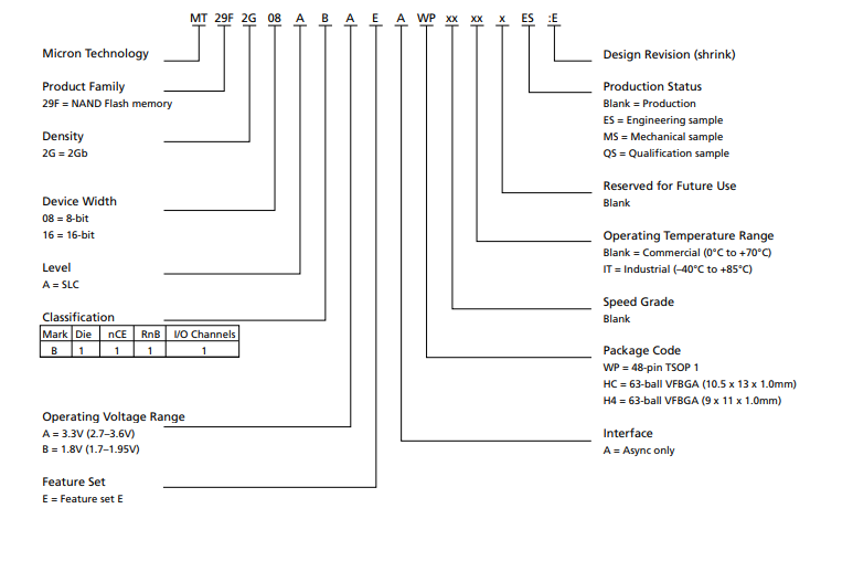
MT29F4G08ABAEAWP:E
MICRON/镁光
TSOP
21+/22+
48