


新洁能NCE7560K N通道增强型功率MOSFET
地区:广东 深圳
认证:
无
图文详情
产品属性
相关推荐
深圳黄金树科技有限公司代理美国福斯特FIRST,无锡新洁能股份有限公司NCEPOWER功率产品,江苏捷捷微JJM可控硅 等二三极,肖特基 LOWVF值电子元件器 本公司长期有库存 ,无锡新洁能股份有限公司,NCE7560K TO-252原装正品,欢迎来电咨询合作
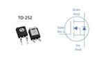
NCE N-Channel Enhancement Mode Power MOSFET Product Summary BVDSS typ. 84 V RDS(ON) typ. 6.8 mΩ max. 8.5 mΩ ID 60 A General Description The NCE7560K uses advanced trench technology and design to provide excellent RDS(ON) with low gate charge. It can be used in a wide variety of applications. Features ● VDS=75V;ID=60A@ VGS=10V; RDS(ON)<8.5mΩ @ VGS=10V ● Special process technology for high ESD capability ● Special designed for Convertors and power controls ● High density cell design for ultra low Rdson ● Fully characterized Avalanche voltage and current ● Good stability and uniformity with high EAS ● Excellent package for good heat dissipation Application ● Power switching application ● Hard Switched and High Frequency Circuits ● Uninterruptible Power Supply 100% UIS TESTED! TO-252-2L top view Schematic diagram Package Marking and Ordering Information Device Marking Device Device Package Reel Size Tape width Quantity NCE7560K NCE7560K TO-252-2L - - -
Table 1. Absolute Maximum Ratings (TC=25℃)
Parameter Symbol Value Unit
Drain-Source Voltage (VGS=0V) VDS 75 V
Gate-Source Voltage (VDS=0V) VGS ±20 V
Drain Current (DC) at Tc=25℃ ID (DC) 60 A
Drain Current (DC) at Tc=100℃ ID (DC) 42 A
Drain Current-Continuous@ Current-Pulsed (Note 1) IDM (pluse) 310 A
Peak diode recovery voltage dv/dt 30 V/ns
Maximum Power Dissipation(Tc=25℃) PD 140 W
Derating factor 0.95 W/℃
Single pulse avalanche energy (Note 2) EAS 300 mJ
Operating Junction and Storage Temperature Range TJ,TSTG -55 To 175 ℃

NCE7560K
NCE
TO-252
无铅环保型
贴片式
卷带编带包装
75V
±20 V
60A
300mJ