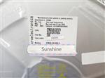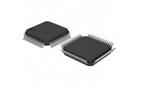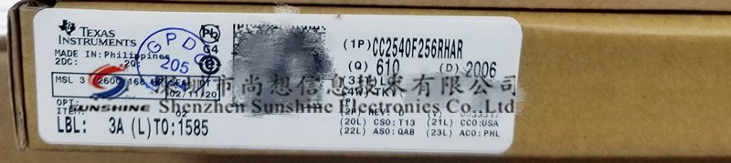
CC2540F256RHAR TI QFN40 射频微控制器 MCU 进口
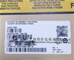
地区:广东 深圳
认证:
无
图文详情
产品属性
相关推荐
CC2540F256RHAR
TI
QFN40
20+
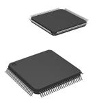
STM32L152VDT6 ST ARM微控制器 MCU QFP 进口
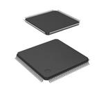
TMS320F28035PAGT TI 德州仪器 LQFP64 进口原装 32位微控制器 MCU
STM32L051C8T6TR ST LQFP48 ARM微控制器 - MCU 16/32-BITS MICROS
ADUC7026BSTZ62-RL ADI LQFP-80 进口原装 ARM微控制器 MCU
TMS320F28067PZT TI LQFP-100 进口原装 32位微控制器 MCU
TMS320F28035PNT TI LQFP80 进口原装 32位微控制器 MCU
TMS320F28034PNT TI LQFP80 进口 32位微控制器 MCU Piccolo Micro
STM32F446RET6意法半导体参数
ARM微控制器STM32F030R8T6参数
STM32F429ZIT6单片机(MCU/MPU/SOC)