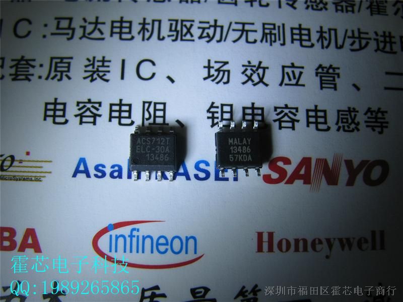


ACS712ELCTR-30A-T全新原装进口货 SOIC8 ACS712ELCTR-30A 假一赔十 可售样品及看货
地区:广东 深圳
认证:
无
图文详情
产品属性
相关推荐

Allegro? ACS712 可为工业、商业和通信系统中的交流或直流电流感测提供经济实惠且精确的解决方案。该器件封装便于客户轻松实施。典型应用包括电动机控制、载荷检测和管理、开关式电源和过电流故障保护。该器件不可用于汽车应用。
该器件具有精确的低偏置线性霍尔传感器电路,且其铜制的电流路径靠近晶片的表面。通过该铜制电流路径施加的电流能够生成可被集成霍尔 IC 感应并转化为成比例电压的磁场。通过将磁性信号靠近霍尔传感器,实现器件精确度优化。精确的成比例电压由稳定斩波型低偏置 BiCMOS 霍尔 IC 提供,该 IC 出厂时已进行精确度编程。
当通过用作电流感测通路的主要铜制电流路径(从引脚 1 和 2,到 3 和 4)的电流不断上升时,器件的输出具有正斜率 (>VIOUT(Q))。该传导通路的内电阻通常是 mΩ,具有较低的功率损耗。铜线的粗细允许器件在可达 5× 的过电流条件下运行。传导通路的接线端与传感器引脚(引脚 5 到 8)之间电气绝缘。这让 ACS712 电流传感器 IC 可用于那些要求电气绝缘却未使用光电绝缘器或其它昂贵绝缘技术的应用。
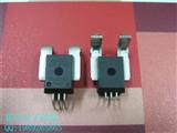
ACS712 采用小型的表面安装 SOIC8 封装。引脚架镀采用 100% 雾锡电镀,可与标准无铅 (Pb) 印刷电路板装配流程兼容。在内部,该器件为无铅产品,倒装法使用当前豁免于 RoHS 的高温含铅焊球除外。器件在出厂装运前已完全校准
主营品牌:美国(Allegro Microsystems) 现货专业分销商 日本SANYO TOSHIBA
步进电机驱动器 旭化成(asahi-kasei)Honeywell,Infineon,Melexis,霍尔
The Allegro®ACS712 provides economical and precise solutions for
AC or DC current sensing in industrial, commercial, and communications systems.
The device package allows for easy implementation by the customer. Typical
applications include motor control, load detection and management, switched-mode
power supplies, and overcurrent fault protection. The device is not intended for
automotive applications. For the automotive grade version, see ACS714.
The device consists of a precise, low-offset, linear Hall sensor circuit with
a copper conduction path located near the surface of the die. Applied current
flowing through this copper conduction path generates a magnetic field which is
sensed by the integrated Hall IC and converted into a proportional voltage.
Device accuracy is optimized through the close proximity of the magnetic signal
to the Hall transducer. A precise, proportional voltage is provided by the
low-offset, chopper-stabilized BiCMOS Hall IC, which is programmed for accuracy
after packaging.
The output of the device has a positive slope (>VIOUT(Q)) when
an increasing current flows through the primary copper conduction path (from
pins 1 and 2, to pins 3 and 4), which is the path used for current sensing. The
internal resistance of this conductive path is 1.2 mΩ typical, providing low
power loss. The thickness of the copper conductor allows survival of the device
at up to 5× overcurrent conditions. The terminals of the conductive path are
electrically isolated from the sensor IC leads (pins 5 through 8). This allows
the ACS712 current sensor IC to be used in applications requiring electrical
isolation without the use of opto-isolators or other costly isolation
techniques.
The ACS712 is provided in a small, surface mount SOIC8 package. The leadframe
is plated with 100% matte tin, which is compatible with standard lead (Pb) free
printed circuit board assembly processes. Internally, the device is Pb-free,
except for flip-chip high-temperature Pb-based solder balls, currently exempt
from RoHS. The device is fully calibrated prior to shipment from the
factory.
ACS712: Fully Integrated, Hall-Effect-Based Linear Current Sensor IC with
2.1 kVRMS Voltage Isolation and a Low-Resistance Current Conductor

供应 CC6920SO-10A SOP-8 CrossChip 电流传感器
供应 LT58-s7 莱姆电流电压传感器 LEM品牌代理
磁阻电流传感器 CSNS300M-002S
供应LEM穿铜排电流传感器HOP1500-SB HOP2000-SB HOP800-SB HTR50-SB
进口ACS758LCB-050B-PFF-T 电流传感器 双向检测直流交流50A
专营Allegro ACS758KCB-150U-PFF-T霍尔电流传感器 进品原装现货,可售样品
Allegro全新原装进口 ACS758ECB-200B-PFF-T霍尔元件电流传感200A
ACS758LCB-100U-PFF-T 电流传感器 ACS758全系列进口全新原装 可售样品及看货
ALLEGRO ACS758KCB-150B-PFF 电流传感器 测150A 全新进口原装现货,可售样品