50 至 200 A 整合式导体传感器 IC
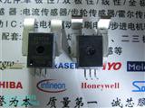
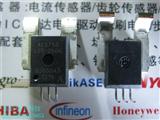
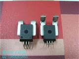
 Allegro CA 和 CB 封装电流传感器 IC 是完全集成的电流传感器解决方案。 它们在单个 IC 封装中整合了主要导体、集中铁磁芯和模拟输出霍尔效应线性装置。 该导体的电阻一般是 100 微欧姆 ,以在感应高达 200 安培的电流时只有极低的功率损耗。这些传感器是汽车级器件,可吸收热量和在极严酷的应用环境中和提供高精度的开放式回路电流感应结果。
Allegro 中级电流器件远小于大型电流变换器,并具有感应直流和交流电流等更多优点。 该封装设计还提供高达 3000 VRMS 的电流隔离,并可在诸多线路侧应用中使用。
ACS758: Thermally Enhanced, Fully Integrated, Hall Effect-Based Linear Current Sensor IC with 100 μΩ Current Conductor
The Allegro® ACS758 family of current sensor ICs provides economical and precise solutions for AC or DC current sensing. Typical applications include motor control, load detection and management, power supply and DC-to-DC converter control, inverter control, and overcurrent fault detection.
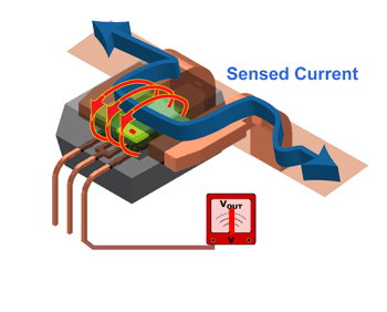
The device consists of a precision, low-offset linear Hall circuit with a copper conduction path located near the die. Applied current flowing through this copper conduction path generates a magnetic field which the Hall IC converts into a proportional voltage. Device accuracy is optimized through the close proximity of the magnetic signal to the Hall transducer. A precise, proportional output voltage is provided by the low-offset, chopper-stabilized BiCMOS Hall IC, which is programmed for accuracy at the factory.
High level immunity to current conductor dV/dt and stray electric fields, offered by Allegro proprietary integrated shield technology, guarantees low output voltage ripple and low offset drift in high-side, high voltage applications.
The output of the device has a positive slope (>VCC / 2) when an increasing current flows through the primary copper conduction path (from terminal 4 to terminal 5), which is the path used for current sampling. The internal resistance of this conductive path is 100 μΩ typical, providing low power loss.
The thickness of the copper conductor allows survival of the device at high overcurrent conditions. The terminals of the conductive path are electrically isolated from the signal leads (pins 1 through 3). This allows the ACS758 family of sensor ICs to be used in applications requiring electrical isolation without the use of opto-isolators or other costly isolation techniques.
The device is fully calibrated prior to shipment from the factory. The ACS758 family is lead (Pb) free. All leads are plated with 100% matte tin, and there is no Pb inside the package. The heavy gauge leadframe is made of oxygen-free copper
Industry-leading noise performance through proprietary amplifier and filter design techniques
Integrated shield greatly reduces capacitive coupling from current conductor to die due to high dV/dt signals, and prevents offset drift in high-side, high voltage applications
Total output error improvement through gain and offset trim over temperature
Small package size, with easy mounting capability
Monolithic Hall IC for high reliability
Ultra-low power loss: 100 μΩ internal conductor resistance
Galvanic isolation allows use in economical, high-side current sensing in high voltage systems
3.0 to 5.5 V, single supply operation
120 kHz typical bandwidth
3 μs output rise time in response to step input current
Output voltage proportional to AC or DC currents
Factory-trimmed for accuracy
Extremely stable output offset voltage
Nearly zero magnetic hysteresis

 Allegro CA 和 CB 封装电流传感器 IC 是完全集成的电流传感器解决方案。 它们在单个 IC 封装中整合了主要导体、集中铁磁芯和模拟输出霍尔效应线性装置。 该导体的电阻一般是 100 微欧姆 ,以在感应高达 200 安培的电流时只有极低的功率损耗。这些传感器是汽车级器件,可吸收热量和在极严酷的应用环境中和提供高精度的开放式回路电流感应结果。
