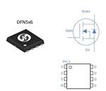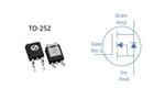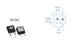
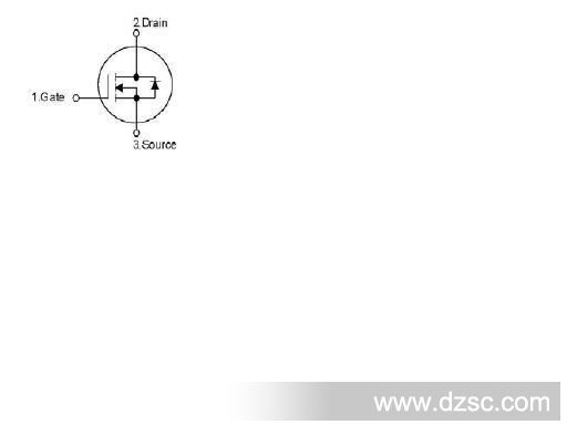
供应 8毫欧 *内阻 电动车控制器用MOSFET 110A 60V
地区:天津 天津市
认证:
无
图文详情
产品属性
相关推荐
供应 8毫欧 *内阻 电动车控制器用MOSFET 110A 60V
Features
■ RDS(on) (Max 0.008 ?) @ VGS=10V
■ Performance and Cost Competitive
■ Advanced Trench Technology
■ Low RDS(on) Minimizes Conduction Loss
■ Low Capacitance Minimizes Driver Loss
■ Optimized Gate Charge Minimizes Switching Loss
General Description
This low voltage Power MOSFET is produced using
advanced high density trench DMOS technology. This lates
technology has been especially designed to minimize
on-state resistance and parasitic capacitance, have a high
rugged avalanche characteristics. These devices are well
suited for high efficiency switching applications、DC/DC
conversion、CPU power delivery and Synchronous
rectification
Symbol Parameter Value Units
VDSS Drain to Source Voltage 60 V
Continuous Drain Current ( @Tc=25
oC ) (Note 3) 110 A
ID
Continuous Drain Current ( @Tc=100
oC ) (Note 3) 70 A
IDM Drain Current Pulsed (Note 1) 380 A
VGS Gate to Source Voltage &plu*n;20 V
EAS Single Pulsed Avalanche Energy (Note 2) 480 mJ
EAR Repetitive Avalanche Energy (Note 1) 15 mJ
Total Power Dissipation ( @Tc=25
oC ) 150 W
PD
Linear Derating Factor 1.0 W/
oC
TSTG, TJ Operating Junction Temperature & Storage Temperature -55 to 175
oC
TL
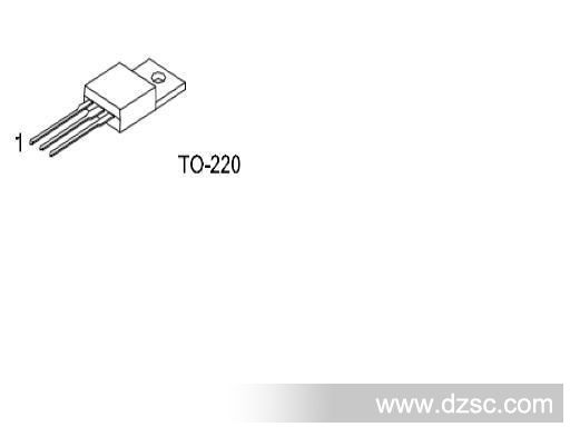
Maximum Lead Tempereture for soldering purpose,
1/8 from Case for 5 seconds
300
oC
Electrical Characteristics (Tc=25oC unless otherwise noted)
Symbol Parameter Test Conditions Min T* Max Units
Off Characteristics
BVDSS Drain-Source Breakdown Voltage VGS=0V, ID=250uA 60 - - V
?BVDSS/
?TJ
Breakdown Voltage Temperature
Coefficience
ID=250uA, referenced to 25oC - 0.03 - V/
oC
VDS=48V, VGS=0V - - 1 uA
IDSS Drain-Source Leakage Current
VDS=48V, VGS=0V, TC=125
oC - - 100 uA
Gate-Source Leakage, Forward VGS=20V, VDS=0V - - 100 nA
IGSS
Gate-Source Leakage, Reverse VGS=-20V, VDS=0V - - -100 nA
On Characteristics
VGS(th) Gate Threshold Voltage VDS=VGS, ID=250uA 2.0 - 4.0 V
RDS(on)
Static Drain-Source On-state
Resistance
VGS=10V, ID=24A - 6.0 8.0 m?
SX
SX3205
*缘栅(MOSFET)
N沟道
增强型
TR/激励、驱动
=
=
=