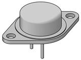
NJW21193G NJW21194G功率晶体管200W PNP
地区:广东 深圳
认证:
无
图文详情
产品属性
相关推荐

The NJW21193G and NJW21194G utilize Perforated Emitter
technology and are specifically designed for high power audio output,
disk head positioners and linear applications.
Features
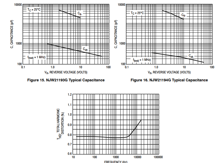
• Total Harmonic Distortion Characterized
• High DC Current Gain
• Excellent Gain Linearity
• High SOA
• These Devices are Pb−Free and are RoHS Compliant
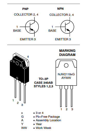
NJW21193G (PNP) NJW21194G (NPN)
 NJW21193G (PNP) NJW21194G (NPN)

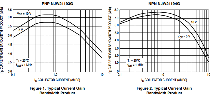
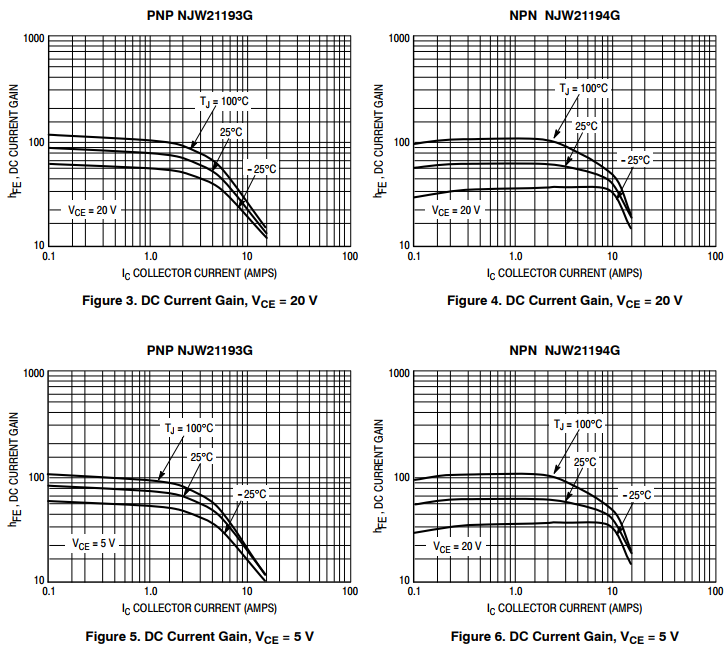
The data of Figure 13 is based on TJ(pk) = 150°C; TC is
variable depending on conditions. At high case
temperatures, thermal limitations will reduce the power than
can be handled to values less than the limitations imposed by
second breakdown.
There are two limitations on the power handling ability of
a transistor; average junction temperature and secondary
breakdown. Safe operating area curves indicate IC − VCE
limits of the transistor that must be observed for reliable
operation; i.e., the transistor must not be subjected to greater
dissipation than the curves indicate.
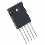
NJW21193G
ON(安森美)
TO-3P
无铅环保型
直插式
散装
大功率
高频
PNP型
250 V
400 V
5 V
1.4 V
16 A
- 65 C+ 150 C
供应MJ15004G 双极晶体管20A 140V 250W PNP
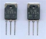
三极管2SA1695 A1695音频管C4468 2SC4468
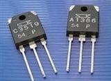
2SA1386 A1386 2SC3519 C3519音频 晶体管
供应MJL21194G 应功率晶体管 TO-264封装
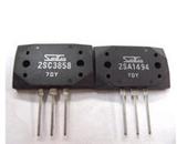
供应2SA1494 2SC3858 TO-3P原装音响发烧对管 三肯/SANKEN品牌 原装进口
MJE15032 NPN, MJE15033 PNP音频放大器
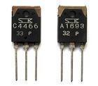
供应全新原装2SA1693 2SC4466 音频功放配对管 A16938/C4466 TO-3P硅外延平面型晶体管(音频和通用)
NPN晶体管2SA1962 A9162 TO-3P 功率放大器
供应MJD350 MJD340 高压电源晶体管应用
音频对管NJL0281DG NJL0302DG TO全新原装