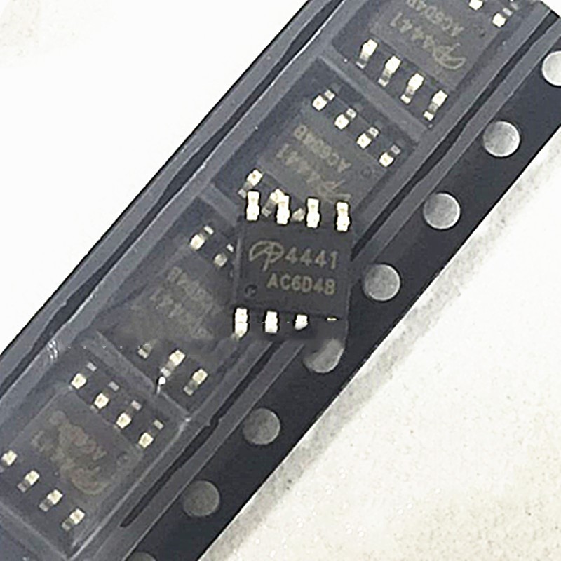

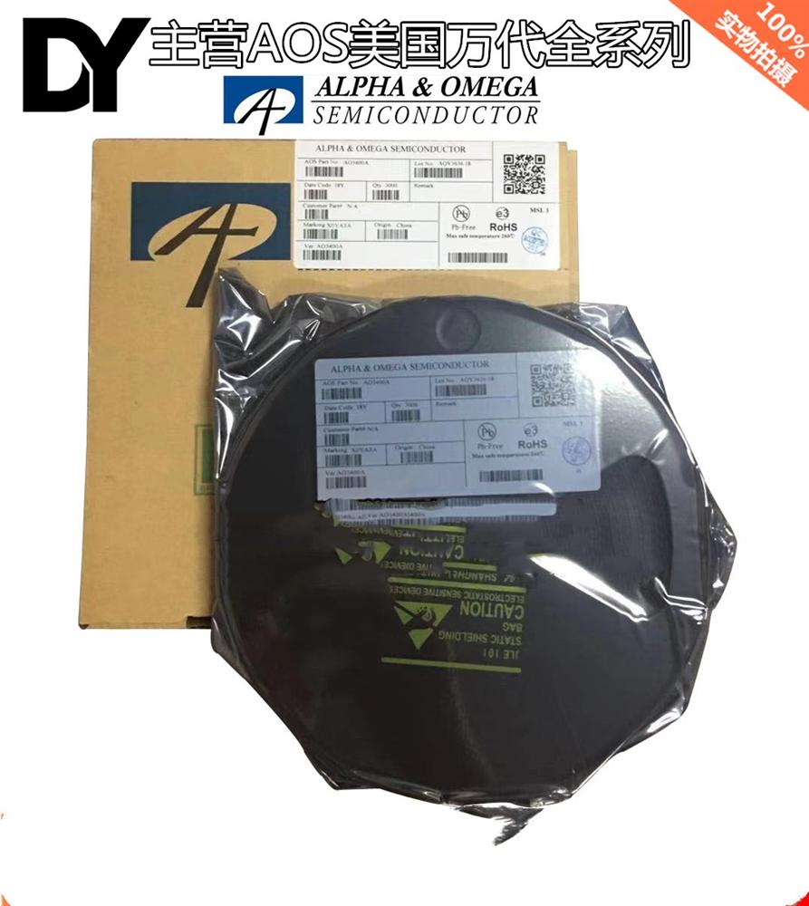

AO4441液晶高压板MOS管 全新现货热卖
地区:广东 深圳
认证:
无
图文详情
产品属性
相关推荐
General Description Product Summary
VDS
ID (at VGS=-10V) -4A
RDS(ON) (at VGS=-10V) < 100mΩ
RDS(ON) (at VGS = -4.5V) < 130mΩ
Symbol
VDS
The AO4441 uses advanced trench technology to provide
excellent RDS(ON), and ultra-low low gate charge. This
device is suitable for use as a load switch or in PWM
applications.
BVDSS -60 V
VDS=-48V, VGS=0V -1
TJ=55°C -5
IGSS ±100 nA
VGS(th) Gate Threshold Voltage -1 -2.1 -3 V
80 100
TJ=125°C 130
102 130 mΩ
gFS 10 S
VSD -0.77 -1 V
IS -4 A
Ciss 930 1120 pF
Coss 85 pF
Crss 35 pF
Rg 7.2 9 Ω
Qg
(10V) 16 20 nC
Qg
(4.5V) 8 10 nC
Qgs 2.5 nC
Qgd 3.2 nC
tD(on) 8 ns
tr 3.8 ns
t 31.5 ns
Electrical Characteristics (TJ=25°C unless otherwise noted)
STATIC PARAMETERS
Parameter Conditions
Drain-Source Breakdown Voltage ID=-250μA, VGS=0V
VGS=-10V, ID=-4A
RDS(ON) Static Drain-Source On-Resistance
IDSS μA
VDS=VGS, ID=-250μA
VDS=0V, VGS= ±20V
Zero Gate Voltage Drain Current
Gate-Body leakage current
mΩ
IS=-1A,VGS=0V
VDS=-5V, ID=-4A
VGS=-4.5V, ID=-3A
Forward Transconductance
Diode Forward Voltage
Turn-On Rise Time
Turn-Off DelayTime
Maximum Body-Diode Continuous Current
Input Capacitance
Output Capacitance
Turn-On DelayTime
DYNAMIC PARAMETERS
VGS=-10V, VDS=-30V, RL=7.5Ω,
R =3Ω
Reverse Transfer Capaci
AO4441
AOS
SOP-8
无铅环保型
贴片式
盒带编带包装
小功率