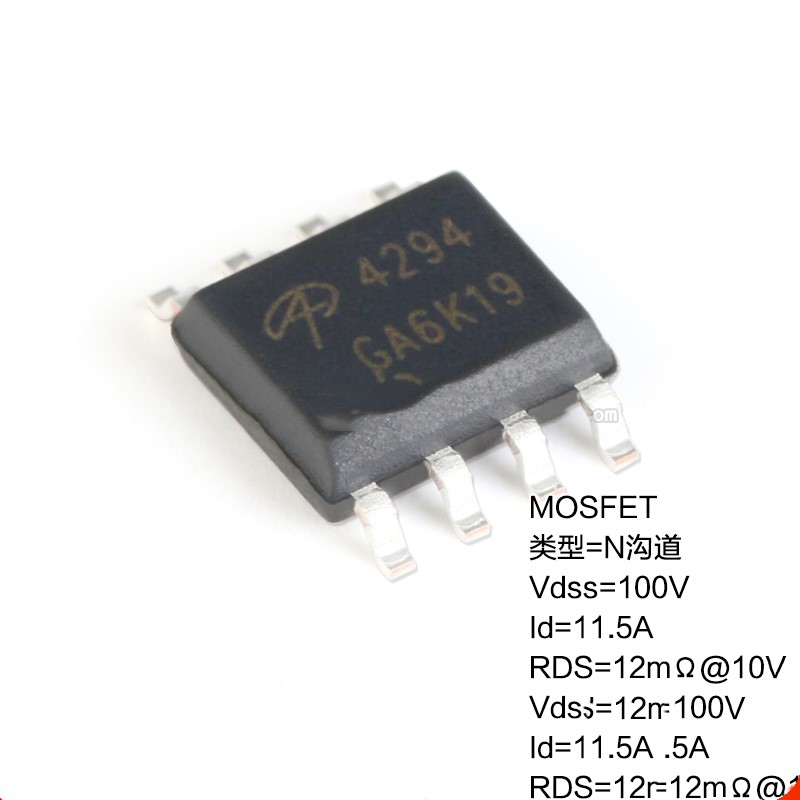


AO4294 液晶高压板MOS管 全新现货热卖
地区:广东 深圳
认证:
无
图文详情
产品属性
相关推荐

General Description Product Summary
VDS
ID (at VGS=10V) 11.5A
RDS(ON) (at VGS=10V) < 12mΩ
RDS(ON) (at VGS=4.5V) < 15.5mΩ
Applications 100% UIS Tested
100% Rg Tested
Symbol
V
• Synchronus Rectification in DC/DC and AC/DC Converters
• Industrial and Motor Drive applications
100
Parameter
Drain-Source Voltage
Absolute Maximum Ratings TA=25°C unless otherwise noted
V
Maximum Units
AO4294 SO-8 Tape & Reel 3000
100V N-Channel MOSFET
Orderable Part Number Package Type Form Minimum Order Quantity
• Trench Power MV MOSFET technology 100V
• Low RDS(ON)
• Low Gate Charge
• Optimized for fast-switching applications

Symbol Min Typ Max Units
BVDSS 100 V
VDS=100V, VGS=0V 1
TJ=55°C 5
IGSS ±100 nA
VGS(th) Gate Threshold Voltage 1.4 1.9 2.4 V
10 12
TJ=125°C 17.5 21
12.5 15.5 mΩ
gFS 45 S
VSD 0.71 1 V
IS 4 A
Ciss 2420 pF
Coss 170 pF
Crss 11 pF
Rg 0.2 0.55 0.9 Ω
Qg
(10V) 33 50 nC
Qg
(4.5V) 15 25 nC
Qgs 7 nC
Qgd 4 nC
tD(on) 8 ns
tr 3 ns
tD(off) 25 ns
tf 4 ns
Reverse Transfer Capacitance
VGS=0V, VDS=50V, f=1MHz
VDS=VGS, ID=250μA
Output Capacitance
Forward Transconductance
IS=1A,VGS=0V
VDS=5V, ID=11.5A
VGS=10V, ID=11.5A
VDS=0V, VGS=±20V
Maximum Body-Diode Continuous Current
Input Capacitance
Gate-Body leakage current
Turn-Off DelayTime
Turn-Off Fall Time
VGS=10V, VDS=50V, RL=4.35Ω,
RGEN=3Ω
Diode Forward Voltage
DYNAMIC PARAMETERS
VGS=4.5V, ID=9.5A
Turn-On Rise Time
Gate Source Charge
Gate Drain Charge
Total Gate Charge
SWITCHING PARAMETERS
Turn-On DelayTime
mΩ
VGS=10V, VDS=50V, ID=11.5A
Total Gate Charge
Electrical Characteristics
AO4294
AOS
SOP-8
无铅环保型
贴片式
卷带编带包装
小功率