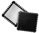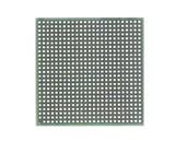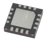

LFXP2-8E-6FTN256I FPGA
地区:广东 深圳
认证:
无
图文详情
产品属性
相关推荐
LFXP2-8E-6FTN256I
FPGA - 现场可编程门阵列 8K LUTs 201 I/O Inst on DSP 1.2V -6 Spd
Introduction LFXP2-8E-6FTN256I
LatticeXP2 devices combine a Look-up Table (LUT) based FPGA fabric with non-volatile Flash cells in an architecture referred to as flexiFLASH.
The flexiFLASH approach provides benefits including instant-on, infinite reconfigurability, on chip storage with FlashBAK embedded block memory and Serial TAG memory and design security. The parts also support Live Update technology with TransFR, 128-bit AES Encryption and Dual-boot technologies.
Architecture Overview LFXP2-8E-6FTN256I
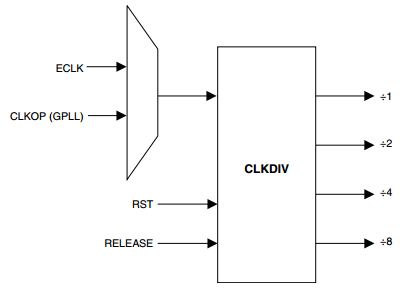
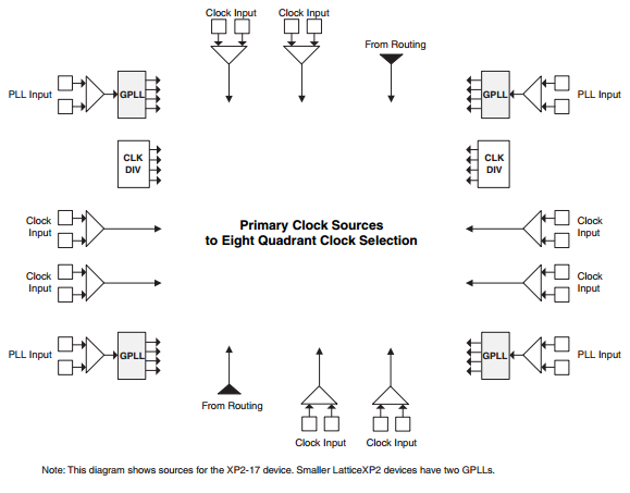
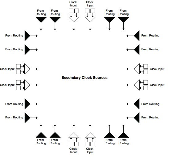
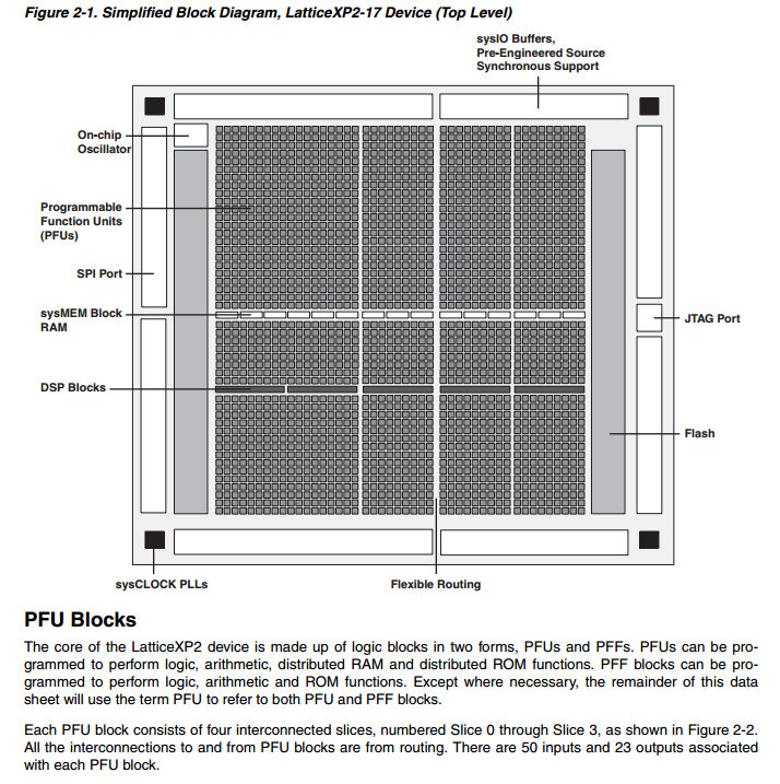
Each LatticeXP2 device contains an array of logic blocks surrounded by Programmable I/O Cells (PIC). Interspersed between the rows of logic blocks are rows of sysMEM™ Embedded Block RAM (EBR) and a row of sysDSP™ Digital Signal Processing blocks as shown in Figure 2-1.
Features LFXP2-8E-6FTN256I
flexiFLASH™ Architecture
• Instant-on
• Infinitely reconfigurable
• Single chip
• FlashBAK™ technology
• Serial TAG memory
• Design security
Flexible I/O Buffer
• sysIO™ buffer supports:
– LVCMOS 33/25/18/15/12; LVTTL
– SSTL 33/25/18 class I, II
– HSTL15 class I; HSTL18 class I, II
– PCI
– LVDS, Bus-LVDS, MLVDS, LVPECL, RSDS
Pre-engineered Source Synchronous Interfaces
• DDR / DDR2 interfaces up to 200 MHz
• 7:1 LVDS interfaces support display applications
• XGMII
: 1.2 V
: - 40 C
: + 100 C
: 18 kbit
: 221 kbit
: 239 kbit