供应W25N01GVZEIGS 原装 NAND FLASH
地区:广东 深圳
认证:
无
图文详情
产品属性
相关推荐
W25N01GVZEIGS 原装 NAND FLASH
3V 1G-BIT SERIAL SLC NAND FLASH MEMORY WITH DUAL/QUAD SPI BUFFER READ & CONTINUOUS READ
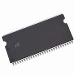
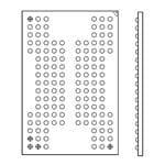
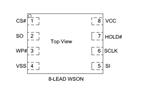
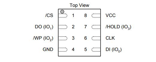
W25N01GV is offered in an 8-pad WSON 8x6-mm (package code ZE), a 16-pin SOIC 300-mil (package code SF), and two 24-ball 8x6-mm TFBGA (package code TB & TC) packages as shown in Figure 1a-c respectively. Package diagrams and dimensions are illustrated at the end of this datasheet.
W25N01GVZEIGS 原装 NAND FLASH 的技术参数:
制造商 | Winbond |
产品种类 | NOR闪存 |
商标 | Winbond |
产品类型 | NOR Flash |
子类别 | Memory & Data Storage |
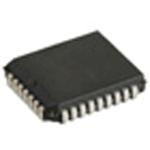
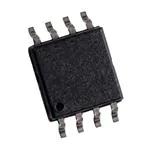
封装 | WSON-8-EP(6.1x8) |
W25N01GVZEIGS 原装 NAND FLASH 的描述:
The W25N01GV (1G-bit) Serial SLC NAND Flash Memory provides a storage solution for systems with limited space, pins and power. The W25N SpiFlash family incorporates the popular SPI interface and the traditional large NAND non-volatile memory space. They are ideal for code shadowing to RAM, executing code directly from Dual/Quad SPI (XIP) and storing voice, text and data.
The device operates on a single 2.7V to 3.6V power supply with current consumption as low as 25mA active and 10μA for standby. All W25N SpiFlash family devices are offered in space-saving packages which were impossible to use in the past for the typical NAND flash memory. The W25N01GV 1G-bit memory array is organized into 65,536 programmable pages of 2,048-bytes each.
The entire page can be programmed at one time using the data from the 2,048-Byte internal buffer. Pages can be erased in groups of 64 (128KB block erase). The W25N01GV has 1,024 erasable blocks. The W25N01GV supports the standard Serial Peripheral Interface (SPI), Dual/Quad I/O SPI: Serial Clock, Chip Select, Serial Data I/O0 (DI), I/O1 (DO), I/O2 (/WP), and I/O3 (/HOLD).
SPI clock frequencies of up to 104MHz are supported allowing equivalent clock rates of 208MHz (104MHz x 2) for Dual I/O and 416MHz (104MHz x 4) for Quad I/O when using the Fast Read Dual/Quad I/O instructions. The W25N01GV provides a new Continuous Read Mode that allows for efficient access to the entire memory array with a single Read command. This feature is ideal for code shadowing applications.
A Hold pin, Write Protect pin and programmable write protection, provide further control flexibility. Additionally, the device supports JEDEC standard manufacturer and device ID, one 2,048-Byte Unique ID page, one 2,048-Byte parameter page and ten 2,048-Byte OTP pages. To provide better NAND flash memory manageability, user configurable internal ECC, bad block management are also available in W25N01GV.
百分百 全新 原包原装原盒 可含税(深圳 香港可交),欢迎前来询问
MT29F64G08CBABAWP固带 10K 23+
KLM8G1GETF-B041 10K 23+
KLMBG2JETD-B041 10K 23+
KLMAG1JETD-B041 10K 23+
K4E6E304EC-EGCG 10K 23+
K4B4G1646E-BCNB 10K 23+
K4F6E3S4HM-MGCJ 10K 23+
K4AAG165WA-BCWE 10K 23+
K4B4G0846E-BCNB 10K 23+
H5TC4G83BFR-PBA 95 17+
H26M41204HPR 5 20+
SDTNRGAMA-008G 35 21+
K4UBE3D4AA-MGCL 10K 23+
K4UBE3D4AB-MGCL 10K 23+
K4U6E3S4AA-MGCR 10K 23+


W25N01GVZEIGS
Winbond
WSON
23+
无铅/环保
AM29F010B-55JF 全新原装
MT25QL256ABA1EW7-0SIT 全新原装 NAND FALSH
MT25QL256ABA8ESF-0SIT TR 全新原装 NAND FLASH
MT29F2T08EMLCEJ4-T:C NAND FLASH 闪存
供应MT25QL128ABB1ESE-0AUT 全新原装 NAND FLASH
MT29F64G08CBABAWP:B 原装 NAND FLASH
供应DS35M1GA-IBR 原装 NAND FLASH
MT25QL128ABA1ESE-0SIT 全新原装
原装MT29F2G01ABAGDWB-IT:G NAND FLASH
FBNL74A61KSBABWP-12AL(PFB29)原装NAND FLASH