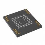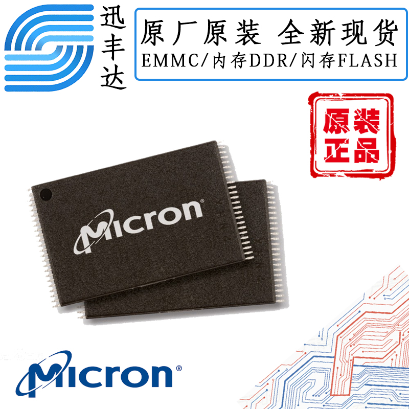


MT41K512M16HA-125:A 原装LPDDR3
地区:广东 深圳
认证:
无
图文详情
产品属性
相关推荐
MT41K512M16HA-125:A 原装LPDDR3
IC DRAM 8GBIT PARALLEL 96FBGA
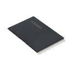
SDRAM - DDR3L 存储器 IC 8Gb(512M x 16) 并联 800 MHz 13.5 ns 96-FBGA(9x14)
|
类别 |
存储器 |
|
制造商 |
Micron Technology Inc. |
|
存储器类型 |
易失 |
|
存储器格式 |
DRAM |
|
技术 |
SDRAM - DDR3L |
|
存储容量 |
8Gb(512M x 16) |
|
存储器接口 |
并联 |
|
时钟频率 |
800 MHz |
|
访问时间 |
13.5 ns |
|
电压 - 供电 |
1.283V ~ 1.45V |
|
电源电流(max) |
88 mA |
|
工作温度 |
0°C ~ 95°C(TC) |
|
安装类型 |
表面贴装型 |
|
外包装 |
TAPE ON REEL |
|
供应商器件封装 |
96-FBGA(9x14) |
DDR3 SDRAM uses a double data rate architecture to achieve high-speed operation.
The double data rate architecture is an 8n-prefetch architecture with an interface designed to transfer two data words per clock cycle at the I/O pins. A single read or write
operation for the DDR3 SDRAM effectively consists of a single 8n-bit-wide, four-clockcycle data transfer at the internal DRAM core and eight corresponding n-bit-wide, onehalf-clock-cycle data transfers at the I/O pins.
The differential data strobe (DQS, DQS#) is transmitted externally, along with data, for
use in data capture at the DDR3 SDRAM input receiver. DQS is center-aligned with data
for WRITEs. The read data is transmitted by the DDR3 SDRAM and edge-aligned to the
data strobes.
The DDR3 SDRAM operates from a differential clock (CK and CK#). The crossing of CK
going HIGH and CK# going LOW is referred to as the positive edge of CK. Control, command, and address signals are registered at every positive edge of CK. Input data is registered on the first rising edge of DQS after the WRITE preamble, and output data is referenced on the first rising edge of DQS after the READ preamble.


MT41K512M16HA-125:A
MICRON/镁光
FBGA
D9STQ
无铅/环保