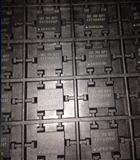

供应K4T1G164QF-BCF7原装进口 K4T1G164QF-BCF7单价用途
地区:广东 深圳
认证:
无
图文详情
产品属性
相关推荐
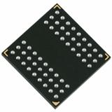
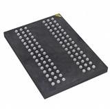
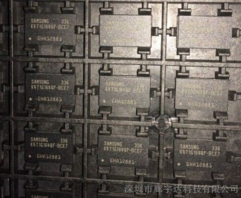
K4T1G164QF-BCF7
SAMSUNG
K4T1G164QF-BCF7
BGA
2015
请来电
供应K4T1G084QF-BCF7 单价 K4T1G084QF-BCF7原装进口
供应K4S511632D-UC75原装进口 K4S511632D-UC75单价用途
供应K4S561632N-LC75 原装进口 K4S561632N-LC75单价 用途
供应K4X1G323PE-8GC6 单价 K4X1G323PE-8GC6原装进口
供应K4T1G084QE-HCF8 单价 K4T1G084QE-HCF8原装进口
供应K4T1G084QF-BCF7 原装进口 K4T1G084QF-BCF7单价用途
供应 MT46H128M16LFDD-48 IT:C​ 存储器 IC
供应MT48LC16M16A2FG-75:D MICRON原装SDR
供应MT48LC16M16A2P-7E IT:D MICRON原装SDR
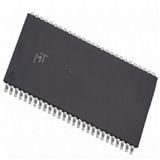
K4B1G1646E-HCKO SAMSUNG原装DDR3 现货供应