Reference design for
SST ATA-Disk Chip into 8051 microcontroller
Application note
Ab
STract: this application note introduces the hardware and firmware of reference design for SST ATA-Disk Chip SST58SD/LDxxx into SST FlashFlex51 SST89C54/58 (8051 compatible microcontroller).
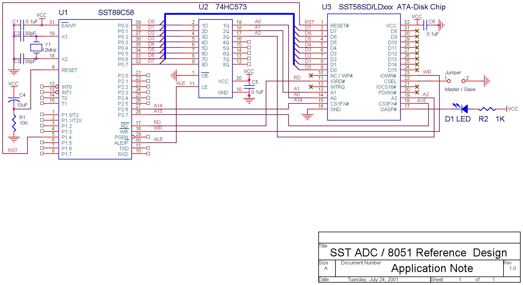
1. Hardware connections:
Please reference to attached schematic diagram for hardware connections.
SST ATA-Disk Chip (ADC) SST58SD/LDxxx only supports one working mode, ie. ATA/IDE mode, all control signals are connected based on Table 2-8, Page 14 on datasheet. After executed Set Feature Command to enable 8-bit data transfers, all higher 8 bit data bus ( D8-D15) are don’t care and can be No Connect. RESET# (pin1) is optional, it can be tied up to Vcc if not used. After
power-up, ADC will automatically be reset internally, it doesn’t need external reset input. But it’s a good practice to connect RESET# to one of I/O pins such as P1.4, in case ADC is out of control for any unknown reasons, host
MCU has capability to reset ADC. DASP# is connected to an emitting diode through a resistor to Vcc,
LED provides user a visibility of ADC’s internal operation. When ADC is active busy on operation, LED will be on. Please be noted that master/slave selection at CSEL pin won’t take effect until Next reset, in other words, if you change the jumper setting of master/slave selection, you MUST reset ADC once.
If your application system expands any other I/O or data memory, please modify the reference design: (1)change CS3FX# to Vcc, (2)connect the output of address decoder to CS1FX#. When both CS1FX# and CS3FX# are high, ADC is de-selected and be standby state, all data bus are in high-z. When CS1FX# is low, ADC is selected and be operational. So CS1FX# acts as Chip Select (/CS) in most common peripherals.
2. Firmware design guide:
It’s important to know that ATA/IDE standard doesn’t permit access only one byte at a time to its media such as HDD or ADC, firmware must read or write data sector by sector, 1 sector has 512 bytes of data, system design engineer must design data buffer to support random access to ADC. Reference design uses the secondary block (4Kbytes x 8bit) of on-chip flash in SST89C54/58 as data buffer.
After power-up or external reset, ADC is default to be 16-bit operation. As SST89C54/58 is 8-bit MCU, firmware must enable 8-bit operation by Set Features Command, please reference to page 32 on datasheet.
If ADC is set as Slave, other than Master, you need to change the bit4 in Drive/Head Register to be 1 when writing Command to ADC, see page 17 on datasheet.
After power-on or reset, ADC will be ready to read / write operation after 200ms (typical), 500ms (maximum), see page 1 under Start Up Time in Features on datasheet.
3. Conclusion:
It’s easy to modify this reference design to any other embedded controllers as long as you follow above design guidelines.
4. Schematic diagram:
5. 8051 Source code:
; all commands supported by ADC.
ChkPwr Equ 0E5h ; 98h
Diagnostic Equ 90h
Format Equ 50h
Identify Equ 0ECh
Idle Equ 0E3h ; 97h
IdleImm Equ 0E1h ; 95h
Initialize Equ 91h
ReadBuf Equ 0E4h
ReadLong Equ 22h ; 23h
ReadMulti Equ 0C4h
ReadSctr Equ 20h ; 21h
ReadVerify Equ 40h ; 41h
Recalibrate Equ 10h ; 1xh
Seek Equ 70h ; 7xh
SetFeature Equ 0EFh
SetMulti Equ 0C6h
Sleep Equ 0E6h ; 99h
Standby Equ 0E2h ; 96h
StandbyImm Equ 0E0h ; 94h
WriteBuf Equ 0E8h
WriteLong Equ 32h ; 33h
WriteMulti Equ 0C5h
WriteSctr Equ 30h ; 31h
WriteVerify Equ 3Ch
;=============================================================
; ADC Drive Register Set definitions
Data_Reg Equ 8000h ; Data Register for read / write
Error_Reg Equ 8001h ; Error Register, read only
Features Equ 8001h ; features Register, write only
Sectr_Cnt Equ 8002h ; Sector Count Register ( R / W )
Sectr_No Equ 8003h ; Sector Number Register, or LBA0:7 ( R / W )
Cylinder_Low Equ 8004h ; Cylinder Low Register or LBA8:15 ( R / W )
Cylinder_Hi Equ 8005h ; Cylinder High Register or LBA16:23 ( R / W )
Drv_Head Equ 8006h ; Drive Head Register ( R / W )
Status Equ 8007h ; Status Register, read only
Command Equ 8007h ; Command Register, write only
Alt_Status Equ 4006h ; Alternate Status Register, read only,
; reading Alt_Status doesn't clear interrupt pending flag. Not used in this demo.
Device_Ctrl Equ 4006h ; Device Control Register, write only. Not used in this demo.
Drive_Addrs Equ 4007h ; Drive Address Register, read only. Not used in this demo.
;=================================================================
; SST FlashFlex51 microcontroller related SFR's definition
SFCF DATA 0B1H ; SuperFlash Configuration
SFCM DATA 0B2H ; SuperFlash Command
SFAL DATA 0B3H ; SuperFlash Address Low
SFAH DATA 0B4H ; SuperFlash Address High
SFDT DATA 0B5H ; SuperFlash Data
SFST DATA 0B6H ; SuperFlash Status
WDTC DATA 0C0H ; Watchdog Timer Control
WDTD DATA 86H ; Watchdog Timer Data/Reload
;=================================================================
; constant definition
FlashAddrs Equ 0F800h ; start address to store data from ADC
;===========================================
org 0000h
ljmp start
org 0100h
start: clr P1.4 ; reset ADC
nop
nop
nop
nop
setb P1.4
mov r4, #5 ; delay 0.5 second
loadr5: mov r5, #200 ; delay 0.1 second
loadr6: mov r6, #250 ; delay 0.5ms for 12MHz crystal
djnz r6, $
djnz r5, loadr6
djnz r4, loadr5
acall Enable8bit ; First of all, enable 8 bits operation!
;========================================
orl SFCF, #40h ; IAPEN=1
mov SFAH, #high(FlashAddrs)
mov SFAL, #low(FlashAddrs)
mov B, #8 ; erase 8 sectors (512 bytes)
;========================================
erase: mov SFCM, #0Bh ; sector erase!
acall Done?
mov a, SFAL
add a, #64 ; 64 bytes / sector in Block 1 of SST89C54/58
mov SFAL, a
mov a, SFAH
addc a, #0
mov SFAH, a
djnz B, erase
anl SFCF, #0BFh ; disable IAP
;========================================
main: acall Write_Sctr
acall Read_Sctr
acall Compare
jb F0, fail
clr P1.4 ; indicates successful operations.
setb P1.5
sjmp $
fail: clr P1.5 ; flags failed comaprison.
setb P1.4
sjmp $
;========================================
Function: acall Busy
mov dptr, #Sectr_Cnt
mov a, R2 ; R2 is Sector Count
movx @dptr, a
mov dptr, #Sectr_No
mov a, R3 ; R3 contains LBA0:7
movx @dptr, a
mov dptr, #Cylinder_Low
mov a, R4 ; R4 contains LBA8:15
movx @dptr, a
mov dptr, #Cylinder_Hi
mov a, R5 ; R5 contains LBA16:23
movx @dptr, a
mov dptr, #Drv_Head
mov a, R6 ; R6 contains LBA24:27
anl a, #00001111b
orl a, #11100000b ; bit4=0 as MASTER, 1 as Slave; bit6=1, enable LBA.
movx @dptr, a
mov dptr, #command
mov a, R7 ; R7 is command code.
movx @dptr, a
ret
;========================================
Busy: mov dptr, #status
movx a, @dptr
jb acc.7, Busy
jb acc.0, errors
; jnb acc.6, Busy
clr a ; acc=0 when successful
clr C ; C=0, ADC is not busy (BUSY=0) and no error (ERR=0)
ret ; and is ready to accept commands (RDY=1)
errors: mov dptr, #Error_Reg
movx a, @dptr
setb C ; C=1 flags error codes contained in ACC register
ret
;========================================
WaitDRQ: mov dptr, #status
movx a, @dptr
jb acc.7, WaitDRQ ; if BUSY=1, then WaitDRQ
jnb acc.3, WaitDRQ ; if DRQ=0, then WaitDRQ
jb acc.0, errors ; if ERR=1, then read errors code and set flag C
; jnb acc.6, WaitDRQ
clr a
clr C ; C=0, ADC is BUSY=0, DRQ=1, ERR=0.
ret
;========================================
Done?: mov a, SFST
jb acc.2, Done?
ret
;========================================
Enable8bit: acall Busy
mov dptr, #Features
mov a, #01h ; enable 8 bit data transfer
movx @dptr, a
mov dptr, #Drv_Head
mov a, #11100000b ; bit4=0 as MASTER, 1 as Slave ; bit6=1, enable LBA
movx @dptr, a
mov dptr, #COMMAND
mov a, #SetFeature ; #0EFh
movx @dptr, a
ret
;========================================
Write_Sctr: mov R2, #1 ; write 1 sector at a time.
mov R3, #0Ah ; suppose LBA to be 000000Ah
mov R4, #0
mov R5, #0
mov R6, #0
mov R7, #WriteSctr
acall Function
acall WaitDRQ
acall Write512
ret
;========================================
Write512: mov R0, #high(message) ; get the higher address of message
mov R1, #low(message) ; get the lower address of message
mov R7, #2 ; 512 bytes = 2 * 256
mov B, #0
write: mov dph, R0 ; get the address
mov dpl, R1
clr a
movc a, @a+dptr ; get the data in message
inc dptr ; point to next byte in message
mov R0, dph ; save the address
mov R1, dpl
mov DPTR, #Data_Reg ; point to ADC
movx @dptr, a ; write 1 byte data into ADC
djnz B, write
djnz R7, write ; write all 512 bytes to ADC
ret
;========================================
Read_Sctr: mov R2, #1 ; read 1 sector at a time.
mov R3, #0Ah ; suppose LBA to be 000000Ah
mov R4, #0
mov R5, #0
mov R6, #0
mov R7, #ReadSctr
acall Function
acall WaitDRQ
acall Read512
ret
;========================================
; read 1 sector of 512 bytes data and write into flash on chip of SST FlashFlex51 MCU
Read512: mov R7, #2 ; 512 bytes = 2 * 256
mov B, #0
mov dptr, #Data_Reg
mov SFAH, #high(FlashAddrs)
mov SFAL, #low(FlashAddrs)
orl SFCF, #40h ; set IAPEN=1 to enable IAP
read: movx a, @dptr ; read 1 byte data from ADC
mov SFDT, a ; program into on-chip flash
mov SFCM, #0Eh ; issue Byte-Program command
acall Done? ; wait until done
mov a, SFAL ; adjust the address of flash
add a, #1
mov SFAL, a
mov a, SFAH
addc a, #0
mov SFAH, a
djnz B, read
djnz R7, read
anl SFCF, #0BFh ; disable IAP
ret
;========================================
Compare: mov dptr, #message ; point to message
mov SFAH, #high(FlashAddrs)
mov SFAL, #low(FlashAddrs)
orl SFCF, #40h ; IAPEN=1
clr F0
mov R7, #2
mov B, #0
verify: clr a
movc a, @a+dptr ; get original data in message
inc dptr
mov SFCM, #0Ch ; issue BYTE-VERIFY command
nop
xrl a, SFDT ; SFDT contains data in flash, these data come from ADC
jz skip
setb F0 ; set flag F0 (PSW.5) if any discrepancy.
skip: mov a, SFAL ; increase the address of flash
add a, #1
mov SFAL, a
mov a, SFAH
addc a, #0
mov SFAH, a
djnz B, verify
djnz R7, verify
anl SFCF, #0BFh ; disable IAP
ret
;========================================================================
message: DB "This demo program demonstrates how easy to design "
DB "SST ATA-Disk Chip into SST FlashFlex51 embedded microcontroller. "
DB "After you understand how to use the basic WriteSector and ReadSector "
DB "functions, it's easy to try any others."
DB "The hardware connection between ADC and MCU is also very simple,"
DB "just like you expand any I/O or data memory in your application system. "
DB "After power-on, ADC is default to be 16 bit operation as all EIDE "
DB "standards, firmware needs enable 8 bit operation before "
DB "further write / read operation."
end