内广视角及良好的色彩饱和度是OLED显示器的主要优点,它在这方面远胜过液晶显示器等其它技术;除此之外,OLED显示器也是一种自发光技术,因此不但不需要背光照明,还能提供比液晶显示器更快的响应时间以支持多媒体应用。目前市场上的OLED材料有两种,分别是小分子和发光聚合物;相较于标准LED,这两种技术的电路参数都很类似,它们的发光强度是由LED顺向偏压电流决定,液晶显示器的像素亮度则是由加在液晶像素的电压决定。
OLED显示器的另一项优点是它能使用现有的基板技术,这和薄膜晶体管(TFT)液晶显示器的基板技术完全相同,主动矩阵OLED显示器可以使用非晶硅(a-Si)或低温多晶硅(LTPS)的TFT基板。
现有OLED技术的主要挑战之一是它的寿命时间,这项限制源自于RGB色彩的衰减速度并不相同,特别是当大部份显示内容为白色时,它需要这三种原色同时发出相同的亮度。受到这些色彩限制的影响,单色显示器就成为市场上早出现的显示器,全彩显示器只用于在产品寿命期限的多数时间内会将显示器关掉的应用。
TI 公司的TPS65137 是有源矩阵 OLED (AMOLED)电源解决方案,包括一个采用LDO作为后稳压器的升压转换器,输入电压从2.3V到5.5V,具有极好的线瞬态稳压功能,输出电压1%,低噪音,输出电流200mA,固定4.6V正输出电压,数字可编程负输出电压可低至-5.2V,具有短路保护和热关断,主要用在有源矩阵 OLED(AMOLED)。本文介绍了TPS65137主要特性,方框图以及典型应用电路。
The TPS65137 consists of a boost converter using a LDO as post regulator. The output voltage of the boost converter is regulated to operate the internal LDO above its dropout voltage maintaining best line and load regulation of OUTP. The internal LDO disconnects OUTP during shutdown and allows regulation of the output when the input voltage is higher than OUTP. The LDO minimizes the output voltage ripple of OUTP. The negative output uses a buck boost converter topology operating in DCM (Discontinuous Conduction Mode) providing superior line regulation. In order to adjust the output voltage of the negative converter a digital interface can be used to program the output voltage. To achieve high efficiency over the entire load current range the device reduces the switching frequency with the load current using its internal voltage controlled oscillator (VCO)。 Since the boost converter output CB is post regulated by the integrated LDO (Low Dropout Regulator) the output voltage ripple is minimized and the line transient response is at its best. Because of this topology the operation mode of the boost converter has minimum effect on the output voltage ripple observed on OUTP. The boost converter, as well as the negative converter operate in peak current mode using the VCO (Voltage Controlled Oscillator) while operating in DCM (Discontinuous Conduction Mode)。 When entering CCM (Continuous Conduction Mode) the converter operates in peak current control using fixed off time control.
TPS65137主要特性:
2.3 V to 5.5 V Input Voltage Range
1% Output Voltage Accuracy Vpos
Excellent Line Transient Regulation
Low Noise Operation
200 mA Output Current
Fixed 4.6 V Positive Output Voltage
Digitally Programmable Negative Output Voltage Down to –5.2V
–4.9V Default Value for Vneg
Advanced Power Save Mode
Short Circuit Protection
Thermal Shutdown
TPS65137A High impedance output in shutdown
3×3 mm 10 Pin QFN Package
TPS65137应用:
Active Matrix OLED Power Supply
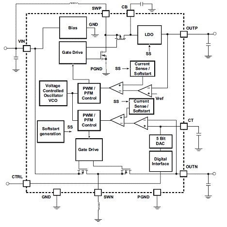
图1。TPS65137功能方框图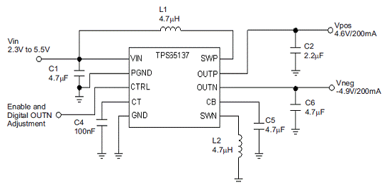
图2。TPS65137典型应用电路图
免责声明: 凡注明来源本网的所有作品,均为本网合法拥有版权或有权使用的作品,欢迎转载,注明出处。非本网作品均来自互联网,转载目的在于传递更多信息,并不代表本网赞同其观点和对其真实性负责。