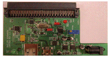
ISP1506评估板为设计者提供了评估ISP1506的特性,以及进行系统级的确认和测试.本文介绍了ISP1504评估板的主要性能,连接器和详细的应用电路图.
The ISP1506 is a 4-bit bidirectional UTMI+ Low Pin Interface (ULPI) transceiver, which provides a Hi-Speed Universal Serial Bus (USB) analog front-end solution to Application-Specific Integrated Circuits (ASICs) and Field Programmable Gate Arrays (FPGAs) to implement as a Hi-Speed USB host, peripheral or OTG device.
The ISP1506 evaluation (eval) board allows you to evaluate the features of the ISP1506 for performance measurement and functionality characterization. The eval board also allows the ULPI Transceiver and Macrocell Tester (T&MT) interface to be connected to a USB link to validate the transceiver.
Fig 1 shows the ISP1506 eval board.

2.1 功能
Fully complies with Universal Serial Bus Specification Rev. 2.0
On-chip 1.5 kΩ pull-up resistor on DP and 15 kΩ pull-down resistors on DP and DM; optional external 1.5 kΩ low-speed pull-up resistor on DM provided on-board
On-chip 45 Ω resistors on DP and DM for high-speed termination
All UTMI+ static signals are accessed using register map
60 MHz clock out (4-bit DDR data interface that clocks on both the rising and falling edges of the clock), can be configured to drive 60 MHz from the USB link on the same pin
Supports full-speed and low-speed UTMI+ serial interface
Supports high-speed, full-speed and low-speed disconnect detection
4-bit DDR data bus that allows USB packet transaction and register access
Supports UTMI+ OTG interface with an internal 50 mA charge pump, or an external VBUS switch or charge pump; an external solution must be used for VBUS current requirements higher than 50 mA.
2.2 连接器
USB connectors: standard-A, standard-B and mini-AB
ULPI through T&MT connector
Input power connector.
2.3 电源
The board power can be directly supplied from an external power supply or from a link through the T&MT connector.
The VBUS power supply is generated from the on-chip charge pump or from the link through the T&MT connector.

图1.ULPI T&MT卡方框图

图2.ISP1406评估板电路图.

图3.ISP1406评估板电路图(2).
表1.ISP1406评估板元器件清单(BOM):


免责声明: 凡注明来源本网的所有作品,均为本网合法拥有版权或有权使用的作品,欢迎转载,注明出处。非本网作品均来自互联网,转载目的在于传递更多信息,并不代表本网赞同其观点和对其真实性负责。