


DDR存储MT46V128M8P-6T IT:A
地区:广东 深圳
认证:
无
图文详情
产品属性
相关推荐
MT46V128M8P-6T IT:A MT46V128M8P-6T IT:A MT46V128M8P-6T IT:A MT46V128M8P-6T IT:A
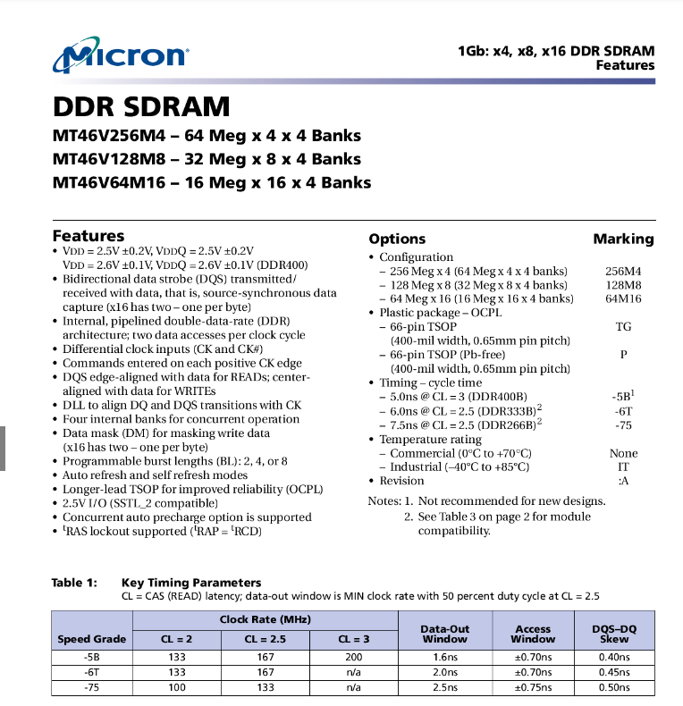
Features
• V DD = 2.5V ±0.2V, V DD Q = 2.5V ±0.2V
V DD = 2.6V ±0.1V, V DD Q = 2.6V ±0.1V (DDR400)
• Bidirectional data strobe (DQS) transmitted/
received with data, that is, source-synchronous data
capture (x16 has two – one per byte)
• Internal, pipelined double-data-rate (DDR)
architecture; two data accesses per clock cycle
• Differential clock inputs (CK and CK#)
• Commands entered on each positive CK edge
• DQS edge-aligned with data for READs; center-
aligned with data for WRITEs
• DLL to align DQ and DQS transitions with CK
• Four internal banks for concurrent operation
• Data mask (DM) for masking write data
(x16 has two – one per byte)
• Programmable burst lengths (BL): 2, 4, or 8
• Auto refresh and self refresh modes
• Longer-lead TSOP for improved reliability (OCPL)
• 2.5V I/O (SSTL_2 compatible)
• Concurrent auto precharge option is supported
•
t RAS lockout supported ( t RAP = t RCD)
Notes: 1. Not recommended for new designs.
2. See Table 3 on page 2 for module
compatibility.
Options Marking
• Configuration
– 256 Meg x 4 (64 Meg x 4 x 4 banks) 256M4
– 128 Meg x 8 (32 Meg x 8 x 4 banks) 128M8
– 64 Meg x 16 (16 Meg x 16 x 4 banks) 64M16
• Plastic package – OCPL
– 66-pin TSOP
(400-mil width, 0.65mm pin pitch)
TG
– 66-pin TSOP (Pb-free)
(400-mil width, 0.65mm pin pitch)
P
• Timing – cycle time
– 5.0ns @ CL = 3 (DDR400B) -5B 1
– 6.0ns @ CL = 2.5 (DDR333B) 2 -6T
– 7.5ns @ CL = 2.5 (DDR266B) 2 -75
• Temperature rating
– Commercial (0?C to +70?C) None
– Industrial (–40°C to +85°C) IT
• Revision :A


DRAM
DDR
tsop66
2.3V ~ 2.7V
1Gb