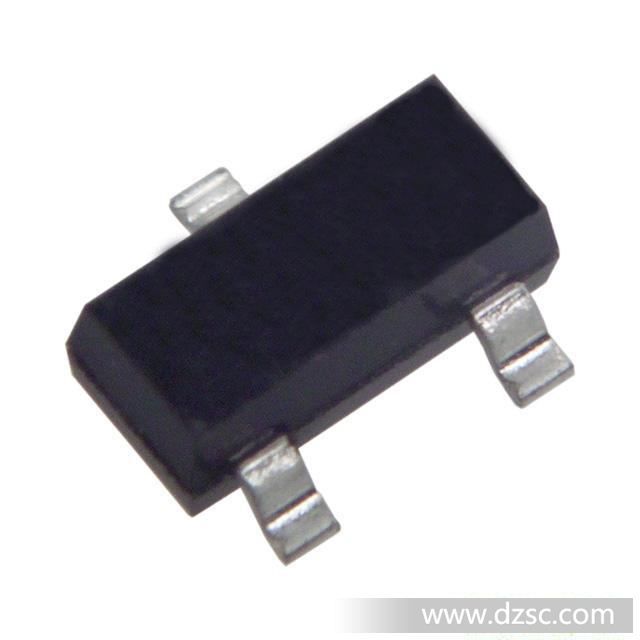


*现货供应 MOS晶体管BSS84
地区:广东 东莞
认证:
无
图文详情
产品属性
相关推荐
*现货供应 MOS晶体管BSS84
BSS84
P-CHANNEL ENHANCEMENT MODE FIELD EFFE*
TRANSISTOR
Features
c183 Low On-Resistance
c183 Low Gate Threshold Voltage
c183 Low Input Capacitance
c183 Fast Switching Speed
c183 Low Input/Output Leakage
Maximum Ratings
@ T
A
= 25c176C unless otherwise specified
Characteristic Symbol BSS84 Units
Drain-Source Voltage VDSS -50 V
Drain-Gate Voltage R
GS
c163 20Kc87 VDGR -50 V
Gate-Source Voltage Continuous VGSS c17720 V
Drain Current (Note 1) Continuous ID -130 mA
Total Power Dissipation (Note 1) Pd 300 mW
Thermal Resistance, Junction to Ambient Rc113JA 417 c176C/W
Operating and Storage Temperature Range Tj,TSTG -55 to 150 c176C
c183 Case: SOT-23, Molded Plastic
c183 Case material - UL Flammability Rating 94V-0
c183 Moisture sensitivity: Level 1 per J-STD-020A
c183 Terminals: Solderable per MIL-STD-202,
Method 208
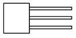
c183 Terminal Connections: See Diagram
c183 Marking (See Page 2): K84
c183 Ordering & Date Code Information: See Page 2
c183 Weight: 0.008 grams (approx.)
Mechanical Data
A
E
J
L
TOP VIEW
M
B C
H
G
D
K
D
G S
Electrical Characteristics
@ T
A
= 25c176C unless otherwise specified
Characteristic Symbol Min T* Max Unit Test Condition
OFF CHARA*ERISTICS (Note 2)
Drain-Source Breakdown Voltage BVDSS -50 c190c190V VGS = 0V, ID = -250?A
Zero Gate Voltage Drain Current IDSS
c190
c190
c190
c190
c190
c190
-15
-60
-100
?A
?A
nA
V
DS
= -50V, V
GS
= 0V, T
J
= 25c176C
V
DS
= -50V, V
GS
= 0V, T
J
= 125c176C
V
DS
= -25V, V
GS
= 0V, T
J
= 25c176C
Gate-Body Leakage IGSS c190c190c17710 nA V
GS
= c17720V, V
DS
= 0V
ON CHARA*ERISTICS (Note 2)
Gate Threshold Voltage VGS(th) -0.8 c190 -2.0 V VDS =VGS, ID = -1mA
Static Drain-Source On-Resistance RDS (ON) c190c19010 c87 VGS = -5V, ID = 0.100A
Forward Transconductance gFS .05 c190c190S VDS = -25V, ID = 0.1A
DYNAMIC CHARA*ERISTICS
Input Capacitance Ciss c190c19045 pF
V
DS
= -25V, V
GS
= 0V
f = 1.0MHz
Output Capacitance Coss c190c19025 pF
Reverse Transfer Capacitance Crss c190c19012 pF
SWITCHING CHARA*ERISTICS
Turn-On Delay Time tD(ON) c190 10 c190 ns
V
DD
= -30V, I
D
= -0.27A,
R
GEN
= 50c87,V
GS
= -10V
Turn-Off Delay Time tD(OFF) c190 18 c190 ns
Note: 1. Device mounted on FR-4 PCB, 1 inch x 0.85 inch x 0.062 inch; pad layout as shown on Diodes Inc. suggested pad layout
document AP02001, which can be found on our website at https://www.diodes.com/datasheets/ap02001.pdf.
2. Short duration test pulse used to minimize self-heating effect.
Source
Gate
Drain
SOT-23
Dim Min Max
A 0.37 0.51
B 1.20 1.40
C 2.30 2.50
D 0.89 1.03
E 0.45 0.60
G 1.78 2.05
H 2.80 3.00
J 0.013 0.10
K 0.903 1.10
L 0.45 0.61
M 0.085 0.180
c97 0c176 8c176
All Dimensions in mm
PHILIPS/Fairchild/长电
BSS84
结型(JFET)
P沟道
增强型
AM/调幅
SMD(SO)/表面封装
P-FET硅P沟道
20(V)
1(V)
0.1(pF)
20(dB)
3(mA)
2(mW)