存储器AT93*6
地区:广东 深圳
认证:
无
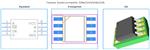
图文详情
产品属性
相关推荐
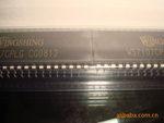
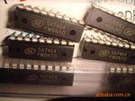
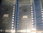
| 品牌:ATMEL/爱特梅尔 | 型号:AT93*6DN | 封装:SOP/SOP |
| 批号:2010 | 制作工艺:半导体集成 | 导电类型:单*型 |
| 规格尺寸:3.9(mm) | 工作温度:-40~125(℃) | 静态功耗:30(mW) |
| 类型:存储器 |
可擦可编程序只读存储器
Features
• Low-voltage and Standard-voltage Operation
– 2.7 (VCC = 2.7V to 5.5V)
– 1.8 (VCC = 1.8V to 5.5V)
• User-selectable Internal Organization
– 1K: 128 x 8 or 64 x 16
– 2K: 256 x 8 or 128 x 16
– 4K: 512 x 8 or 256 x 16
• Three-wire Serial Interface
• 2 MHz Clock Rate (5V)
• Self-timed Write Cycle (10 ms max)
• High Reliability
– Endurance: 1 Million Write Cycles
– Data Retention: 100 Years
• Automotive Grade, Extended Temperature and Lead-Free/Halogen-Free
Devices Available
• 8-lead PDIP, 8-lead JEDEC SOIC, 8-lead EIAJ SOIC, 8-lead MAP, 8-lead TSSOP,
and 8-ball dBGA2 Packages
Description
The AT93*6/56/66 provides 1024/2048/4096 bits of serial electrically erasable pro-
grammable read-only memory (EEPROM), organized as 64/128/256 words of 16 bits
each (when the ORG pin is connected to VCC), and 128/256/512 words of 8 bits each
(when the ORG pin is tied to ground). The device is optimized for use in many indus-
trial and commercial applications where low-power and low-voltage operations are
essential. The AT93*6/56/66 is available in space-saving 8-lead PDIP, 8-lead
JEDEC SOIC, 8-lead EIAJ SOIC, 8-lead MAP, 8-lead TSSOP, and 8-lead dBGA2
packages.
The AT93*6/56/66 is enabled through the Chip Select pin (CS) and accessed via a
three-wire serial interface consisting of Data Input (DI), Data Output (DO), and Shift
Clock (SK). Upon receiving a Read instruction at DI, the address is decoded and the
data is clocked out serially on the DO pin. The Write cycle is completely self-timed,
and no separate Erase cycle is required before Write. The Write cycle is only enabled
when the part is in the Erase/Write Enable state. When CS is brought high following
the initiation of a Write cycle, the DO pin outputs the Ready/Busy status of the part.
The AT93*6/56/66 is available in 2.7V to 5.5V and 1.8V to 5.5V versions.