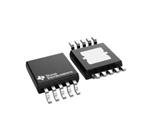
供应原装TI逻辑IC,CD54HC73F3A 触发器/锁存器/寄存器 > J-K 触发器 >
地区:广东 深圳
认证:
无
图文详情
产品属性
相关推荐
The ’HC73 and CD74HCT73 utilize silicon gate CMOS technology to achieve operating speeds equivalent to LSTTL parts. They exhibit the low power consumption of standard CMOS integrated circuits, together with the ability to drive 10 LSTTL loads.
These flip-flops have independent J, K, Reset and Clock inputs and Q and Q\ outputs. They change state on the negative-going transition of the clock pulse. Reset is accomplished asynchronously by a low level input. This device is functionally identical to the HC/HCT107 but differs in terminal assignment and in some parametric limits.
The HCT logic family is functionally as well as pin compatible with the standard LS logic family.
 1A at VOL, VOH
Data sheet acquired from Harris Semiconductor
CD54HC73F3A
TI(德州仪器)