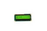
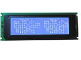
供应12864液晶模块
地区:广东 深圳
认证:
无
图文详情
产品属性
相关推荐
Contents
1. SPECIFICATIONS
1.1 Features
1.2 Mechanical Specifications
1.3 Absolute Maximum Ratings
1.4 DC Electrical Characteristics
1.5 Backlight & LED Characteristics
2. MODULE STRU*URE
2.1 Counter Drawing
2.2 Interface Pin Description
2.3 Timing Characteristics
2.4 Instruction Table
2.5 PROGRAM
3. QUALITY ASSURANCE SYSTEM
Quality Assurance Flow Chart
4. PRECAUTION RELATING PRODU* HANDLING
4.1 Safety
4.2 Handling
4.3 Storage
4.4 Terms of Warranty
1. SPECIFICATIONS
1.1 Features
|
Item |
Standard Value |
|
Display T*e |
128*64 Dots |
|
LCD T*e |
STN,Positive |
|
Driver Condition |
LCD Module : 1/64Duty |
|
Viewing Direction |
6 O’clock |
|
Backlight T*e |
Yellow/Green LED B/L |
|
Interface |
8Bits data bus |
|
Driver IC |
KS0108,KS0107 |
1.2 Mechanical Specifications
|
Item |
Standard Value |
Unit |
|
Outline Dimension |
70.0 (W) * 93.0(L) * 13.5 (H)(Max) |
mm |
|
Viewing Area |
40.0 (W) * 72.00 (L) |
mm |
|
Active Area |
33.24 (W) * 66.52(L) |
mm |
|
Dot Size |
0.48 (W) * 0.48(L) |
mm |
|
Dot Pitch |
0.52(W) * 0.52(L) |
mm |
1.3 Absolute Maximum Ratings
|
Item |
Symbol |
Condition |
Min. |
Max. |
Unit |
|
System Power Supply Voltage |
VDD |
- |
-0.3 |
5.0 |
V |
|
LCD Driver Supply Voltage |
VOUTIN |
- |
- |
10.0 |
V |
|
Input Voltage |
VIN |
- |
-0.3 |
VDD + 0.3 |
V |
|
Operating Temperature |
TOP |
- |
-20 |
70 |
°C |
|
Storage Temperature |
TST |
- |
-30 |
80 |
°C |
|
Storage Humidity |
HD |
Ta < |
20 |
90 |
%RH |
1.4 DC Electrical Characteristics
VDD = 5.0V ± 0.2V , GND = 0V , Ta =
|
Item |
Symbol |
Condition |
Min. |
T*. |
Max. |
Unit |
|
Logic Supply Voltage |
VDD |
- |
4.75 |
5.0 |
5.25 |
V |
|
Input High Voltage |
VIH |
- |
0.8VDD |
- |
VDD |
V |
|
Input Low Voltage |
VIL |
- |
GND |
- |
0.3VDD |
V |
|
Output High Voltage |
VOH |
- |
0.7VDD |
- |
VDD |
V |
|
Output Low Voltage |
VOL |
- |
GND |
- |
0.2VDD |
V |
|
LCD Driver Voltage |
VOP |
VOP –GND ( |
|
|
|
V |
|
VOP -GND ( |
9.8 |
10.0 |
- | |||
|
VOP -GND ( |
|
|
|
1.5 Backlight Characteristics
LCD Module with LED Backlight
Electrical / Optical Characteristics
Ta =
|
Item |
Symbol |
Conditions |
Min. |
T*. |
Max. |
Unit |
|
Forward Voltage |
Vf |
If=360mA |
4.0 |
4.1 |
4.2 |
V |
|
Reverse Current |
IR |
If=8v |
|
360 |
|
uA |
|
Average Brightness |
IV |
If=360mA |
568 |
570 |
574 |
cd/m2 |
|
Wavelength (Without LCD) |
λp |
If= |
|
|
|
nm |
|
Luminous Intensity (without LCD) |
IV |
If= |
|
|
|
cd/m2 |
|
Uniformity |
Δ% |
IVMin / IVMax *100% |
75 |
- |
- |
% |
|
Color |
Y/G | |||||
2. MODULE STRU*URE
2.1 Counter Drawing
* See Appendix
2.2 Interface Pin Description
|
Pin No. |
Symbol |
Function |
|
1 |
Vss |
Ground |
|
2 |
VDD |
Power supply input for driver IC (+5.0V). |
|
3 |
VO |
LCD operation voltage test pin. |
|
4 |
D/I |
Data and control register select input H : D0 to D7 are display data. L : D0 to D7 are control data. |
|
5 |
R/W |
Write signal input, active “ L “ |
|
6 |
E |
Enable signal input, active “H”→“ L “ |
|
7 |
DB0 |
Data bus bit 0 |
|
8 |
DB1 |
Data bus bit 1 |
|
9 |
DB2 |
Data bus bit 2 |
|
10 |
DB3 |
Data bus bit 3 |
|
11 |
DB4 |
Data bus bit 4 |
|
12 |
DB5 |
Data bus bit 5 |
|
13 |
DB6 |
Data bus bit 6 |
|
14 |
DB7 |
Data bus bit 7 |
|
15 |
CS1 |
Chip select pin |
|
16 |
CS2 |
Chip select pin |
|
17 |
/R* |
Reset signal input f, active “ L” |
|
18 |
VOUT |
LCD DRIVE VOLTAGE(NEGATIVE) |
|
19 |
A |
Power supply anode input for backlight (5V) |
|
20 |
K |
Power supply cathode input for backlight(GROUND) |
*G12864
*G