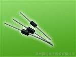
*现货供应 *开关二*管M*D914LT1G
地区:广东 东莞
认证:
无
图文详情
产品属性
相关推荐
*现货供应 *开关二*管M*D914LT1G
M*D914LT1/D
M*D914LT1
Preferred Device
High−Speed Switching
Diode
Features
• Pb−Free Package is Available
MAXIMUM RATINGS
Rating Symbol Value Unit
Reverse Voltage VR 100 Vdc
Forward Current IF 200 mAdc
Peak Forward Surge Current IFM(surge) 500 mAdc
THERMAL CHARA*ERISTICS
Characteristic Symbol Max Unit
Total Device Dissipation
FR−5 Board (Note 1)
TA = 25°C
Derate above 25°C
PD 225
1.8
mW
mW/°C
Thermal Resistance, Junction−to−Ambient
R JA 556 °C/W
Total Device Dissipation
Alumina Substrate (Note 2)
TA = 25°C
Derate above 25°C
PD 300
2.4
mW
mW/°C
Thermal Resistance, Junction−to−Ambient
R JA 417 °C/W
Junction and Storage Temperature
Range
TJ, Tstg −55 to +150 °C
Maximum ratings are those values beyond which device damage can occur.
Maximum ratings applied to the device are individual stress limit values (not
normal operating conditions) and are not valid simultaneously. If these limits are
exceeded, device functional operation is not implied, damage may occur and
reliability may be affected.
ELE*RICAL CHARA*ERISTICS (TA = 25°C unless otherwise noted)
Characteristic Symbol Min Max Unit
OFF CHARA*ERISTICS
Reverse Breakdown Voltage
(IR = 100 Adc)
V(BR) 100 − Vdc
Reverse Voltage Leakage Current
(VR = 20 Vdc)
(VR = 75 Vdc)
IR
−
−
25
5.0
nAdc
Adc
Diode Capacitance
(VR = 0, f = 1.0 MHz)
* − 4.0 pF
Forward Voltage
(IF = 10 mAdc)
VF − 1.0 Vdc
Reverse Recovery Time
(IF = IR = 10 mAdc) (Figure 1)
trr − 4.0 ns
1. FR−5 = 1.0 0.75 0.062 in.
2. Alumina = 0.4 0.3 0.024 in. 99.5% alumina.
Device Package Shipping†
ORDERING INFORMATION
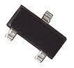
SOT−23
CASE 318
STYLE 8
M*D914LT1 SOT−23 3000/Tape & Reel
MARKING DIAGRAM
1
A*DE
3
CATHODE
Prefe
快恢复二*管
ON/长电
M*D914LT1G
平面型
硅(Si)
SOT-23
塑料封装
*率
中频
橙色
无色透明(T)
圆灯
标准型
100(V)
200(mA)