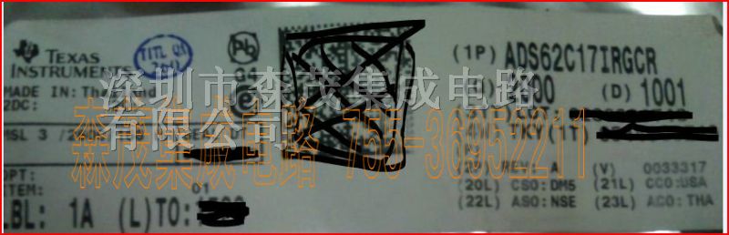


供应德州仪器的*模数转换器集成电路ADS62C17IRG*
地区:广东 深圳
认证:
无
图文详情
产品属性
相关推荐
TI 主页 > 半导体 > 数据转换器 > 模数转换器 > * ADC (>10MSPS) > adss62c17irgct
具有 SNRBoost 的双通道 11 位 200MSPS ADC 集成电路 ADS62C17IRG*
Dual Channel 11 Bit, 200 MSPS ADC with SNRBoost ADS62C17IRG*
数据列表 ADS62C17
产品相片 64-VQFN_ExposedPad
标准包装 250
类别 集成电路 (IC)
家庭 数据采集 - 模数转换器
系列 -
位数 11
采样率(每秒) 200M
数据接口 串行, 并联
转换器数目 2
功率耗散(*大) 1.1W
电压电源 模拟和数字
工作温度 -40°C ~ 85°C
安装类型 表面贴装
封装/外壳 64-VFQFN *焊盘
供应商设备封装 64-VQFN *焊盘 (9x9)
包装 带卷 (TR)
输入数目和类型 2 个差分,单*
说明
ADS62C17 is a dual channel 11-bit, 200 MSPS A/D converter that combines high dynamic performance and low power consumption in a compact 64 QFN package. This makes it well-suited for multi-carrier, wide band-width communications applications.
ADS62C17 uses TI-proprietary SNRBoost technology that can be used to overcome SNR limitation due to quantization noise for bandwidths less than Nyquist (Fs/2). It includes several useful and commonly used di*al functions such as ADC offset correction, gain (0 to 6 dB in steps of 0.5 dB) and gain tuning (in fine steps of 0.001 dB).
The gain option can be used to improve SFDR performance at lower full-scale input ranges. Using the gain tuning capability, each channel’s gain can be set independently to improve channel-to-channel gain matching.
ADS62C17是一个双通道11位,200 MSPS A / D转换,结合在一个紧凑的64 QFN封装的高动态性能和低功耗。这使得它*适合多载波,宽带宽通信应用。
ADS62C17采用TI专有的SNRBoost技术可用于克服信噪比由于量化噪声的带宽小于奈奎斯特(FS / 2)的限制。它包括几个有用的和常用的数码功能,如ADC的偏移校正,增益(0至6分贝步长为0.5分贝)和增益调整(精度0.001分贝)。
增益选项,可用于*在较低的满量程输入范围的SFDR性能。使用增益调整功能,每个通道的增益可以*设置,以*通道对通道增益匹配。
View full Description in Datasheet
特性
Maximum Sample Rate: 200 MSPS
11-bit Resolution with No Missing Codes
90 dBc SFDR at Fin = 10 MHz
79.8 dBFS SNR at 125 MHz IF, 20 MHz BW
using TI proprietary SNRBoost technology
Total Power 1.1 W at 200 MSPS
90 dB Cross-talk
Double Data Rate (DDR) LVDS and Parallel
CMOS Output Options
Programmable Gain up to 6dB for SNR/SFDR Trade-off
DC Offset Correction
Gain Tuning Capability in Fine Steps (0.001 dB)
Allows Channel-to-channel Gain Matching
Supports Input Clock Amplitude Down to
400 mV p-p Differential
Internal and External Reference Support
64-QFN Package (9 mm × 9 mm)
参数
ADS62C15 ADS62C17
Resolution(Bits) 11 11
Sample Rate (max) 125MSPS 200MSPS
# Input Channels 2 2
Interface LVDS, Parallel and Serial SPI Interface LVDS, Parallel and Serial SPI Interface
SNR(dB) 67.2 67
SFDR(dB) 89 85
Power Consumption(T*)(mW) 740 1081
Operating Temperature Range(°C) -40 to 85 -40 to 85
Rating Catalog Catalog
Analog Voltage */DD(Min)(V) 3 3.15
Analog Voltage */DD(Max)(V) 3.6 3.8
Di*al Supply(Min)(V) 3 1.7
Di*al Supply(Max)(V) 3.6 1.9
Architecture Pipeline Pipeline
INL(Max)(+/-L*) 3.5 2.5
SINAD(dB) 67.1 66.9
E*B(Bits) 10.8 10.8
Input Range 2V (p-p) 2V (p-p)
Reference Mode Int and Ext Int and Ext
ADS62C17IRG* /VQFN(RGC)/64
TI (Texas Instruments德州仪器)