图文详情
产品属性
相关推荐
1 Features
1• High-Performance 1:2, 1:3, 1:4, 1:6, 1:8, 1:10,
1:12 LVCMOS Clock Buffer Family
• Very Low Pin-to-Pin Skew < 50 ps
• Very Low Additive Jitter < 100 fs
• Supply Voltage: 3.3 V or 2.5 V
• fmax = 250 MHz for 3.3 V
fmax = 180 MHz for 2.5 V
• Operating Temperature Range: –40°C to 85°C
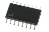
• Available in 8-, 14-, 16-, 20-, 24-Pin TSSOP
Package (All Pin-Compatible)
2 Applications
General-Purpose Communication, Industrial, and
Consumer Applications
3 Description
The CDCLVC11xx is a modular, high-performance,
low-skew, general-purpose clock buffer family from
Texas Instruments.
The entire family is designed with a modular
approach in mind. It is intended to round up TI's
series of LVCMOS clock generators.
Seven different fan-out variations, 1:2 to 1:12, are
available. All of the devices are pin-compatible to
each other for easy handling.
All family members share the same high performing
characteristics such as low additive jitter, low skew,
and wide operating temperature range.
The CDCLVC11xx supports an asynchronous output
enable control (1G) which switches the outputs into a
low state when 1G is low.
The CDCLVC11xx family operates in a 2.5-V and
3.3-V environment and ar

4 Output
250 MHz
2 ns
TSSOP-8
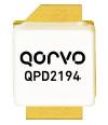
供应QPD2194美国QORVO氮化镓晶体管
LM4890MM/NOPB Texas Instruments 音频放大器 1 Watt Audio Pwr Amp
MAX3490ESA+ RS-422/RS-485 接口 Maxim
525R-03ILF时钟发生器及支持产品 IDT
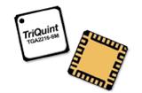
供应TGA2216-SM美国QORVO氮化镓晶体管
61082-041602LF板对板与夹层连接器Amphenol
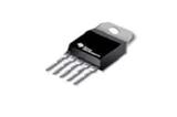
LM2592HVT-5.0/NOPB Texas Instruments 开关稳压器 pwr Cnvtr 150 KHz 2A SD Vtg Reg
SFW4R-1STE1LF FFC & FPC连接器Amphenol
供应AG303-86G美国QORVO氮化镓晶体管
MAX187BCWE+ 模数转换器 - ADC Maxim
