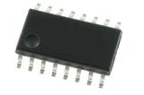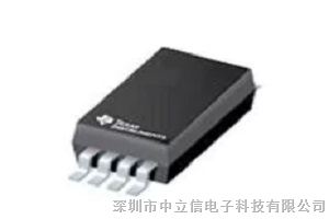

CDCLVC1102PWR Texas Instruments 时钟缓冲器 Lo Jitter,1:2 LVCMOS Fan-out
地区:广东 深圳
认证:
无
图文详情
产品属性
相关推荐
1 Features
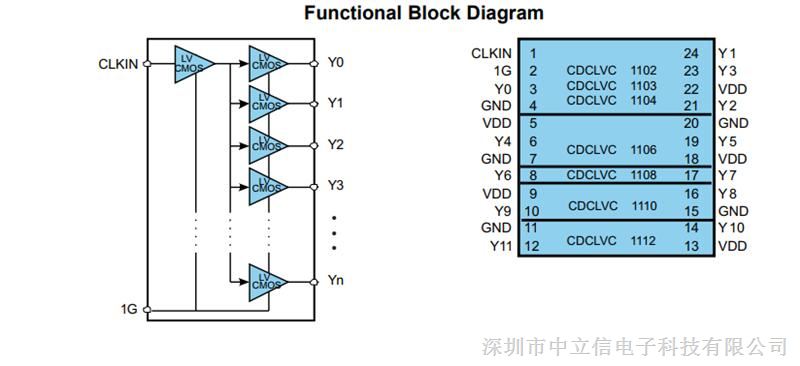
1• High-Performance 1:2, 1:3, 1:4, 1:6, 1:8, 1:10,
1:12 LVCMOS Clock Buffer Family
• Very Low Pin-to-Pin Skew < 50 ps
• Very Low Additive Jitter < 100 fs
• Supply Voltage: 3.3 V or 2.5 V
• fmax = 250 MHz for 3.3 V
fmax = 180 MHz for 2.5 V
• Operating Temperature Range: –40°C to 85°C
• Available in 8-, 14-, 16-, 20-, 24-Pin TSSOP
Package (All Pin-Compatible)
2 Applications
General-Purpose Communication, Industrial, and
Consumer Applications
3 Description
The CDCLVC11xx is a modular, high-performance,
low-skew, general-purpose clock buffer family from
Texas Instruments.
The entire family is designed with a modular
approach in mind. It is intended to round up TI's
series of LVCMOS clock generators.
Seven different fan-out variations, 1:2 to 1:12, are
available. All of the devices are pin-compatible to
each other for easy handling.
All family members share the same high performing
characteristics such as low additive jitter, low skew,
and wide operating temperature range.
The CDCLVC11xx supports an asynchronous output
enable control (1G) which switches the outputs into a
low state when 1G is low.
The CDCLVC11xx family operates in a 2.5-V and
3.3-V environment and are characterized for
operation from –40°C to 85°C.
2 Output
250 MHz
TSSOP-8
2 ns