

TPS22902BYFPR电源开关IC - 配电原裝德州TI
地区:广东 深圳
认证:
无
图文详情
产品属性
相关推荐
1 Features 2 Applications
1• Integrated P-Channel Load Switch • Personal Digital Assistants (PDAs)
• Low Input Voltage: 1 V to 3.6 V • Cellular Phones
• ON-Resistance (Typical Values) • GPS Devices
– rON = 78 mΩ at VIN = 3.6 V • MP3 Players
– rON = 93 mΩ at VIN = 2.5 V • Digital Cameras
– rON = 109 mΩ at V • Peripheral Ports IN = 1.8 V
– r • Portable Instrumentation ON = 146 mΩ at VIN = 1.2 V
• 500 mA Maximum Continuous Switch Current • RF Modules
• Quiescent Current: 82 nA at 1.8 V
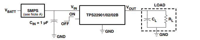
3 Description • Shutdown Current: 44 nA at 1.8 V
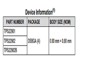
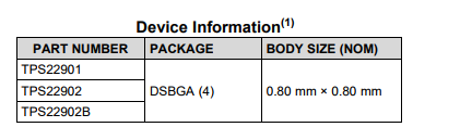
The TPS22901, TPS22902, and TPS22902B are
• Low Control Input Thresholds Enable Use of small, low ON-resistance (rON) load switches with a
1.2-V, 1.8-V, 2.5-V, and 3.3-V Logic controlled turnon. These devices contain a P-channel
• Controlled Slew Rate to Avoid Inrush Currents MOSFET that operates over an input voltage range of
1.0 V to 3.6 V. The switch is controlled by an on/off – tr = 40 μs at VIN = 1.8 V (TPS22901/2)
input (ON), which can interface directly with low–
tr = 220 μs at VIN = 1.8 V (TPS22902B) voltage control signals. In the TPS22902 and
• Quick Output Discharge (TPS22902/2B) TPS22902B, an 88-Ω on-chip load resistor is added
• ESD Performance Tested Per JESD 22 for output quick discharge when the switch is turned
off.
– 2000-V Human Body Model
(A114-B, Class II) The TPS22901, TPS22902, and TPS22902B are
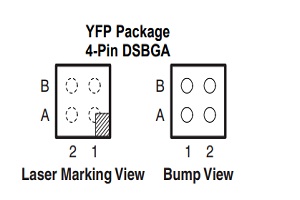
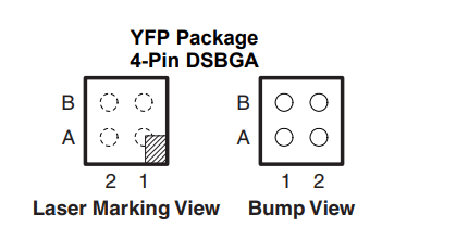
available in a space-saving 4-pin DSBGA (YFP) with – 1000-V Charged-Device Model (C101)
0.4-mm pitch. These devices are characterized for
TPS22902BYFPRTPS22902BYFPRTPS22902BYFPRTPS22902BYFPR
1功能2应用
•集成p通道负载开关•个人数字助理(pda)
•低输入电压:1 V至3.6 V•移动电话
•ON-Resistance(典型值)•GPS设备
——罗恩= 78 mΩVIN = 3.6 V•MP3播放器
——罗恩= 93 mΩVIN = 2.5 V•数码相机
——罗恩= 109 mΩV•周边港口= 1.8 V
- r•便携式仪器在VIN = 146 mΩ= 1.2 V
•500毫安最大连续开关电流•射频模块
•静止电流:1.8 V时为82 nA
关闭电流:44 nA at 1.8 V
TPS22901、TPS22902和TPS22902B是
•低控制输入阈值允许使用小的、低通电阻(rON)负载开关
1.2-V、1.8-V、2.5-V、3.3-V逻辑控制turnon。这些设备包含一个p通道
•控制旋转速度,以避免在输入电压范围内运行的涌流MOSFET
1.0 V至3.6 V。开关的开/关控制- tr = 40μs VIN = 1.8 V(TPS22901/2)
输入(ON),可以直接与低-进行接口
tr = 220μs VIN = 1.8 V(TPS22902B)电压控制信号。在TPS22902和
•快速输出放电(TPS22902/2B)TPS22902B 88Ω芯片上的负载阻抗
•根据JESD 22测试ESD性能,在开关转动时输出快速放电
掉了。
- 2000-V人体模型
(A114-B, II类)TPS22901、TPS22902和TPS22902B
适用于节省空间的4针DSBGA (YFP)与- 1000-V收费设备模型(C101)
0.4毫米。这些装置的特点是
•四脚晶片芯片级DSBGA封装操作在自由空气温度范围内
- 0.8毫米×0.8毫米,0.8毫米,-40°C到85°C。
0.5毫米的高度(YFP)
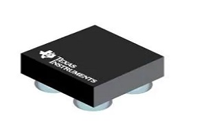
Texas Instruments
电源开关 IC - 配电
1 Output
500 mA
500 mA
95 mOhms
1 V to 3.6 V
480 mW
SMD/SMT
DSBGA-4
33 us
7 us
MAX6864UK29D3S+T 监控电路 Maxim
供应NLB-310美国QORVO氮化镓晶体管
HM2J07PE5128N9LF 硬公制连接器 Amphenol
TPS65270PWPR电源管理 (PMIC)原装TI
MAX813LESA+ 监控电路 Maxim
LM1117MPX-3.3/NOPB Texas Instruments 低压差稳压器 800MA LDO LINEAR REG
TPS71725DCKR低压差稳压器 L-N原装TI
TPS3705-30DR监控电路Processor原装德州TI
TPS650250RHBR电池管理 Power原装德州TI
51722-10400800AALF电源到板Amphenol FCI