图文详情
产品属性
相关推荐
标准包装:25
Features
• Wide Range of Digital and Analog Signal Levels
- Digital . . . . . . . . . . . . . . . . . . . . . . . . . . . . . . 3V to 20V
- Analog. . . . . . . . . . . . . . . . . . . . . . . . . . . . . . . ≤20VP-P
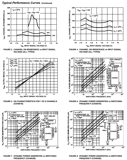
• Low ON Resistance, 125Ω (Typ) Over 15VP-P Signal Input
Range for VDD-VEE = 18V
• High OFF Resistance, Channel Leakage of ±100pA (Typ)
at VDD-VEE = 18V
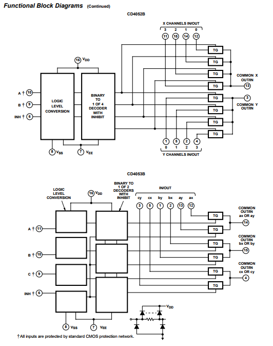
• Logic-Level Conversion for Digital Addressing Signals of
3V to 20V (VDD-VSS = 3V to 20V) to Switch Analog
Signals to 20VP-P (VDD-VEE = 20V)
• Matched Switch Characteristics, rON = 5Ω (Typ) for
VDD-VEE = 15V
• Very Low Quiescent Power Dissipation Under All DigitalControl
Input and Supply Conditions, 0.2μW (Typ) at
VDD-VSS = VDD-VEE = 10V
• Binary Address Decoding on Chip
• 5V, 10V, and 15V Parametric Ratings
• 100% Tested for Quiescent Current at 20V
• Maximum Input Current of 1μA at 18V Over Full Package
Temperature Range, 100nA at 18V and 25oC
• Break-Before-Make Switching Eliminates Channel
Overlap

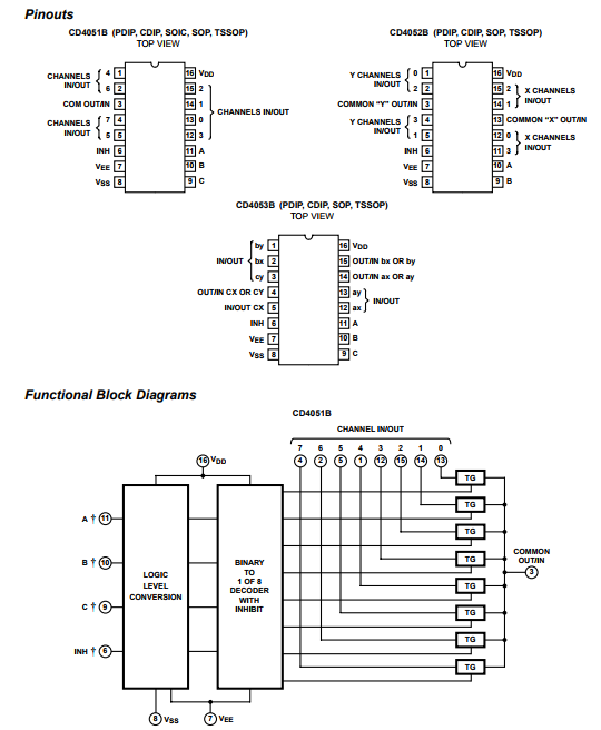
CD4051BF3A, CD4052BF3A,
CD4053BF3A
CD4051BE, CD4052BE,
CD4053BE
CD4051BM, CD4051BMT,
CD4051BM96
CD4053BM, CD4053BMT,
CD4053BM96
CD4051BNSR, CD4052BNSR,
CD4053BNSR
CD4051BPW, CD4051BPWR,
CD4053BPW, CD4053BPWR


CD4052
TI
DIP16
-55°C ~ 125°C
3 V ~ 20 V,±2.5 V ~ 9 V