


NXP 逻辑集成电路 移位寄存器 74HC595D
地区:广东 深圳
认证:
无
图文详情
产品属性
相关推荐
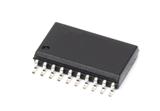
74HC595D

74HC595D
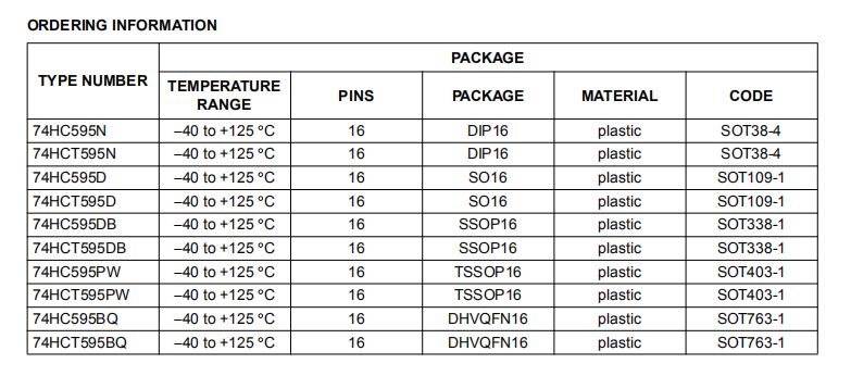
74HC595D
FEATURES
• 8-bit serial input
• 8-bit serial or parallel output
• Storage register with 3-state outputs
• Shift register with direct clear
• 100 MHz (typical) shift out frequency
• ESD protection:
HBM EIA/JESD22-A114-A exceeds 2000 V
MM EIA/JESD22-A115-A exceeds 200 V.
74HC595D
APPLICATIONS
• Serial-to-parallel data conversion
• Remote control holding register.
DESCRIPTION
The 74HC/HCT595 are high-speed Si-gate CMOS devices
and are pin compatible with low power Schottky TTL
(LSTTL). They are specified in compliance with JEDEC
standard no. 7A.
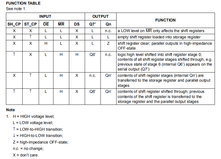
The 74HC/HCT595 is an 8-stage serial shift register with a
storage register and 3-state outputs. The shift register and
storage register have separate clocks.
Data is shifted on the positive-going transitions of the
SH_CP input. The data in each register is transferred to
the storage register on a positive-going transition of the
ST_CP input. If both clocks are connected together, the
shift register will always be one clock pulse ahead of the
storage register.
The shift register has a serial input (DS) and a serial
standard output (Q7’) for cascading. It is also provided
with asynchronous reset (active LOW) for all 8 shift
register stages. The storage register has 8 parallel 3-state
bus driver outputs. Data in the storage register appears at
the output whenever the output enable input (OE) is LOW.
74HC595D
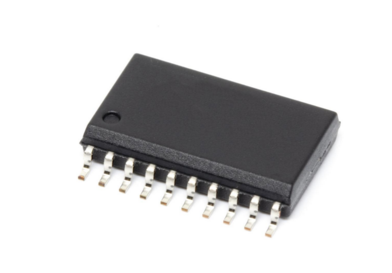
NXP
SOP
19+
环保
2000/盘
中国
黑色