图文详情
产品属性
相关推荐
GMT致新 G5416QS1U QFN4X4-30 22+ 完整的DDR内存电源解决方案
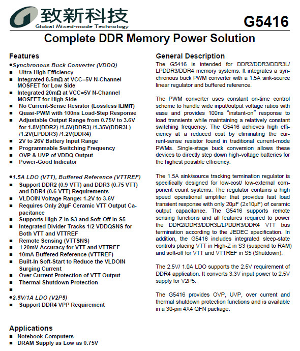
General Description
The G5416 is intended for DDR2/DDR3/DDR3L/
LPDDR3/DDR4 memory systems. It integrates a synchronous
buck PWM converter with a 1.5A sink-source
linear regulator and buffered reference.
The PWM converter uses constant on-time control
scheme to handle wide input/output voltage ratios with
ease and provides 100ns “instant-on” response to
load transients while maintaining a relatively constant
switching frequency. The G5416 achieves high efficiency
at a reduced cost by eliminating the current-
sense resistor found in traditional current-mode
PWMs. Single-stage buck conversion allows these
devices to directly step down high-voltage batteries for
the highest possible efficiency.
The 1.5A sink/source tracking termination regulator is
specifically designed for low-cost/ low-external component
count systems. The regulator contains a high
speed operational amplifier that provides fast load
transient response with only 20μF (2x10μF) of ceramic
output capacitance. The G5416 supports remote
sensing functions and all features required to power
the DDR2/DDR3/DDR3L/LPDDR3/DDR4 VTT bus
termination according to the JEDEC specification. In
addition, the G5416 includes integrated sleep-state
controls placing VTT in High-Z in S3 (suspend to RAM)
and soft-off for VTT and VTTREF in S5 (Shutdown).
The 2.5V/ 1.0A LDO supports the 2.5V requirement of
DDR4 application. It converts 3.3V input power to 2.5V
supply for V2P5.
The G5416 provides OVP, UVP, over current and
thermal shutdown protection functions and is available
in a 30-pin 4X4 QFN package.
G5416QS1U QFN4X4-30 应用原理图:

Features
Synchronous Buck Converter (VDDQ)
Ultra-High Efficiency
Integrated 8.5mΩ at VCC=5V N-Channel
MOSFET for Low Side
Integrated 20mΩ at VCC=5V N-Channel
MOSFET for High Side
No Current-Sense Resistor (Lossless ILIMIT)
Quasi-PWM with 100ns Load-Step Response
Adjustable Output Range from 0.75V to 3.6V
for 1.8V(DDR2) /1.5V(DDR3) /1.35V(DDR3L)
/1.2V(LPDDR3) /1.2V(DDR4)
2V to 26V Battery Input Range
Programmable Switching Frequency
OVP & UVP of VDDQ Output
Power-Good Indicator
1.5A LDO (VTT), Buffered Reference (VTTREF)
Support DDR2 (0.9 VTT) and DDR3 (0.75 VTT)
and DDR4 (0.6 VTT) Requirements
VLDOIN Voltage Range: 1.2V to 3.6V
Requires Only 20μF Ceramic VTT Output Capacitance
Supports High-Z in S3 and Soft-Off in S5
Integrated Divider Tracks 1/2 VDDQSNS for
Both VTT and VTTREF
Remote Sensing (VTTSNS)
±20mV Accuracy for VTT and VTTREF
10mA Buffered Reference (VTTREF)
Built-In Soft-Start to Reduce the VLDOIN
Surging Current
Over Current Protection of VTT Output
Thermal Shutdown Protection
2.5V/1A LDO (V2P5)
Support DDR4 VPP Requirement
Applications
Notebook Computers
DRAM Supply as Low as 0.75V

G5416QS1U
GMT
QFN4X4-30
22+
台湾