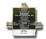
供应GPS天线分配器 ALDCBS1x8
地区:上海 上海市
认证:
无
图文详情
产品属性
相关推荐
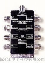
ALDCBS1X8
Technical Product Data
Features
• Amplifier Gain of 14dB
Gain ≥ 13dB
• Extremely Flat Group Delay
Less that 1ns variation
• Phase Matched Outputs
Phase (J1 – J2) < 1.0o
Description
The ALDCBS1X8 GPS Amplified Splitter is a one input, eight output device with 13dB minimum gain. The frequency response covers the GPS L1 & L2 bands with excellent gain flatness. In the normal configuration, one of the splitter RF outputs (J1) passes DC from the connected GPS receiver through the splitter to the antenna, allowing the GPS receiver to power both the antenna and the splitter’s amplifier. The other RF outputs (J2, J3, J4, J5, J6, J7 and J8) are DC loaded with 200Ω resistors to simulate antenna current draw to prevent antenna fault readings from connected GPS receivers.
Electrical Specifications, TA = 250C
|
Parameter |
Conditions |
Min |
Typ |
Max |
Units |
|
Freq. Range |
Ant – Any Output, Unused Outputs - 50Ω |
1.1 |
|
1.7 |
GHz |
|
In/Out Imped. |
Ant, J1, J2, J3, J4, J5, J6, J7, J8 |
|
50 |
|
Ω |
|
Gain |
Ant–Any Output, Unused Outputs- 50Ω |
13 |
14.5 |
16.5 |
dB |
|
Input SWR |
All ports - 50Ω |
|
|
2.0:1 |
- |
|
Output SWR |
All ports - 50Ω |
|
|
1.8:1 |
- |
|
Noise Figure |
Normal Config., Ant – Any Output, Unused Outputs - 50Ω |
|
3.8 |
4.3 |
dB |
|
Gain Flatness |
| L1 – L2 | ; Ant – Any Output, Unused Outputs - 50Ω |
|
0.5 |
1 |
dB |
|
Amplitude Ballance |
| J1 – J2 | ; Ant – Any Output, Unused Outputs - 50Ω |
|
|
0.5 |
dB |
|
Phase Ballance |
Phase (J1 – J2) ; Ant – Any Output, Unused Outputs - 50Ω |
|
|
1.0 |
deg |
|
Isolation |
Normal Config., Adjacent Ports, Ant - 50Ω (see plots) |
10 |
|
|
dB |
|
Group delay Flatness |
τd,max - τd,min : Ant – J1, J2 - 50Ω ; Ant – J2, J1 - 50Ω |
|
|
1 |
ns |
|
Req. DC Input V. |
Non-Network Configuration, DC Input on J1 |
3.6 |
|
15 |
Vdc |
|
Pı dB |
Output Power @1dB Gain Compression (f = 1.5GHZ) |
|
-2.0 |
|
dBm |
|
Current (1) |
Amplifier Current Draw, All ports - 50Ω |
|
|
15 |
mA |
(1). Current draw on input DC port in the non-networked configuration.
Hi-Isolation Option Specifications
Electrical Specifications, TA = 250C
|
Parameter |
Conditions |
Min |
Typ |
Max |
Units |
|
Freq. Range |
Ant – Any Output, Unused Outputs - 50Ω |
1.1 |
|
1.7 |
GHz |
|
In/Out Imped. |
Ant, J1, J2, J3, J4, J5, J6, J7, J8 |
|
50 |
|
Ω |
|
Gain |
Any Output, Unused Outputs - 50Ω |
3 |
4.5 |
6.5 |
dB |
|
Input SWR |
All ports - 50Ω |
|
|
2.0:1 |
- |
|
Output SWR |
All ports - 50Ω |
|
|
1.3:1 |
- |
|
Noise Figure |
Ant – Any Output, Unused Outputs - 50Ω |
|
4.0 |
4.5 |
dB |
|
Gain Flatness |
| L1 – L2 | ; Ant – Any Output, Unused Outputs - 50Ω |
|
0.5 |
1 |
dB |
|
Amplitude Balance |
| J1 – J2 | ; Ant – Any Output, Unused Outputs - 50Ω |
|
|
0.5 |
dB |
|
Phase Balance |
Phase (J1 – J2) ; Ant – Any Output, Unused Outputs - 50Ω |
|
|
1.0 |
deg |
|
Isolation |
Adjacent Ports, Ant - 50Ω (see plots) |
35 |
|
|
dB |
|
Group delay Flatness |
τd,max - τd,min : Ant – J1, J2 - 50Ω ; Ant – J2, J1 - 50Ω |
|
|
1 |
ns |
|
Req. DC Input V. |
Non-Network Configuration, DC Input on J1 |
3.6 |
|
15 |
Vdc |
|
Pı dB |
Output Power 1dB Gain Compression (f=1.5GHz) |
|
-2.0 |
|
dBm |
|
Current (1) |
Amplifier Current Draw, All ports - 50Ω |
|
|
15 |
mA |
(1). Current draw on input DC port in the non-networked configuration.
Available Options
|
Network Power Supply |
||
|
Source Voltage Options |
VOLTAGE INPUT |
STYLE |
|
110VAC |
Transformer (Wall Mount) |
|
|
220 VAC |
Transformer (Wall Mount) |
|
|
240 VAC (United Kingdom) |
Transformer (Wall Mount) |
|
|
Input DC Voltage 9 - 32 VDC |
Military Style Connector |
|
|
Output Voltage Options (1) |
DC VOLTAGE OUT |
MAX CURRENT OUT FOR CORRESPONDING Vout(2) |
|
5 V |
110mA |
|
|
7.5V |
130mA |
|
|
9V |
140mA |
|
|
12V |
170mA |
|
|
15V |
210mA |
|
|
Custom |
TDB |
|
|
Output Port Isolation Options |
||
|
Isolation Options |
Normal Isolation, 10dB min. Output Port – to – Output Port |
|
|
High Isolation, 35dB min. Output Port – to – Output Port |
||
|
Pass/Block DC Options |
||
|
Pass DC(1) |
All Ports Pass DC |
|
|
DC Blocked (1) |
Jx (x=2…8) is DC blocked, Pass DC from J1 to ANT. |
|
|
RF Connector Options |
||
|
Connector Options |
CONNECTOR STYLE |
CHARGE |
|
Type N |
NC |
|
|
Type SMA |
NC |
|
|
Type TNC |
NC |
|
|
Type BNC |
NC |
|
(1). With Network Option, any RF port (input or output) can be DC blocked or can pass the network DC
voltage.
Part Number
N HI AL DCB S1X8- S / 5 / 110
Network Option:
N = Network Option; Blank = No Network
Isolation Option:
HI = Hi Isolation Option; Blank = Normal
DC Options:
DCB = DC Blocked; PDC = Pass DC Connector Options:
N = N type; S = SMA; T = TNC; B = BNC DC Output Voltage:
3.3, 5, 7.5, 9, 12, 15, CXX (Custom: “XX” denotes desired V) Source Voltage:
110 -Transformer, 220 – Transformer, 240 – Transformer, MC – Military DC Connector (User
supplies 9-32 VDC)
Mechanical
Dimensions: Height: 1.3”
Length (not including connectors) Body: 4.5”
Base Plate: 5.25” Width (not including connectors): 2.5”
Weight: 16.2 oz. (459 grams) Operating Temp. Range: -40o to + 75oC
Performance
ALDCBS1X8 (Normal Output Isolation Option):
|
|
Input SWR (Ant. Port) and Frequency Response: Ant. To JX (X=1…8) (Typical, type N connector):
ALDCBS1X8 (Normal Output Isolation Option) (continued):
|
|
Output SWR JX (X=1…8) and Adjacent Output Isolation (J1-J3, J2-J4, etc) (Typical, type N connectors):
ALDCBS1X8 (Normal Output Isolation Option) (continued):
|
|
Opposite Output Isolation (J1-J2,J3-J4, etc) (Typical, type N conn.):
HIALDCBS1X8 (Hi Output Isolation Option) (continued):
|
|
Output SWR (J1, J2, J3, J4) and Adjacent Output Isolation (J1-J3, J2-J4) (Typical, type N connectors):
ALDCBS1X8 (Hi Output Isolation Option) (continued):
|
|
Opposite Output Isolation (J1-J2, J3-J4) (Typical, type N connectors):
ALDCBS1x8
ALDCBS1x8