图文详情
产品属性
相关推荐
Copyright:
Copyright © 2007 Genesys Logic Incorporated.All rights reserved. No part of the materials may be
reproduced in any form or by any means without prior written consent of Genesys Logic, Inc.
Disclaimer:
ALL MATERIALS ARE PROVIDED “AS IS” WITHOUT EXPRESS OR IMPLIED WARRANTY OF ANY
KIND. NO LICENSE OR RIGHT IS GRANTED UNDER ANY PATENT OR TRADEMARK OF
GENESYS LOGIC INC.. GENESYS LOGIC HEREBY DISCLAIMS ALL WARRANTIES AND
CONDITIONS IN REGARD TO MATERIALS, INCLUDING ALL WARRANTIES, IMPLIED OR
EXPRESS, OF MERCHANTABILITY, FITNESS FOR ANY PARTICULAR PURPOSE, AND
NON-INFRINGEMENT OF INTELLECTUAL PROPERTY. IN NO EVENT SHALL GENESYS LOGIC
BE LIABLE FOR ANY DAMAGES INCLUDING, WITHOUT LIMITATION, DAMAGES RESULTING
FROM LOSS OF INFORMATION OR PROFITS. PLEASE BE ADVISED THAT THE MATERIALS
MAY CONTAIN ERRORS OR OMMISIONS. GENESYS LOGIC MAY MAKE CHANGES TO THE
MATERIALS OR TO THE PRODUCTS DESCRIBED THEREIN AT ANY TIME WITHOUT NOTICE.
Revision History
Revision Date Description
1.00 07/07/2005 First Formal release
1.01 09/07/2005 Modify Pin Description, table3.3, p.12
1.02 09/15/2005 Modify HUB Interface ,table3.3 Pin Description, p.12
1.03 12/28/2005 Modify Pin List and Pin Descriptions of EE_CS, EE_DI, EE_SK, p.11~12
1.04 01/19/2006 Add AC Characteristics, Ch6.5, p.26
1.05 03/29/2006 Add Input Voltage for digital I/O(Ovcur1-4,Pself,Reset) pins, p.23
1.06 06/15/2006
Changed GL852-N to GL852
1.GL852 48 Pin Pinout, Pin List, Pin Description, p.10~13
Add GL852 QFN 48PIN
1.07 07/18/2006 Modify GL852 48 Pin QFN Package, p.30
1.08 09/05/2006 Modify Clock and Reset Interface of GL852 48 pin to 64 pin, p.14
1.09 11/03/2006 Modify 93C46 Configuration, Table 5.1, p.22
1.10 12/08/2006 Modify General Description, Ch1, p.7
1.11 03/12/2007 Modify RESET# Setting, Ch5.2.1, p.18
1.12 05/03/2007 Add “TJ” , Table 6.2, p.24
1.13 05/16/2007 Add “θJA”, Table 6.2, p.24
1.14 07/19/2007 Modify PGANG/SUSPND Setting, Ch5.2.2, p.19
TABLE OF CONTENTS
CHAPTER 1 GENERAL DESCRIPTION................................................... 7
CHAPTER 2 FEATURES.............................................................................. 8
CHAPTER 3 PIN ASSIGNMENT ................................................................ 9
3.1 PINOUTS...................................................................................................... 9
3.2 PIN LIST.................................................................................................... 12
3.3 PIN DESCRIPTIONS ................................................................................... 13
CHAPTER 4 BLOCK DIAGRAM.............................................................. 15
CHAPTER 5 FUNCTION DESCRIPTION............................................... 16
5.1 GENERAL.................................................................................................. 16
5.2 CONFIGURATION AND I/O SETTINGS....................................................... 18
CHAPTER 6 ELECTRICAL CHARACTERISTICS............................... 24
6.1 MAXIMUM RATINGS................................................................................. 24
6.2 OPERATING RANGES................................................................................ 24
6.3 DC CHARACTERISTICS ............................................................................ 24
6.4 POWER CONSUMPTION ............................................................................ 26
6.5 AC CHARACTERISTICS ............................................................................ 27
CHAPTER 7 PACKAGE DIMENSION..................................................... 28
CHAPTER 8 ORDERING INFORMATION ............................................ 31
CHAPTER 1 GENERAL DESCRIPTION
GL852 is Genesys Logic’s brand new Hub solutions which fully comply with Universal Serial Bus
Specification Revision 2.0. This series includes GL852.
GL852 embeds an 8-bit RISC processor to manipulate the control/status registers and respond to the requests
from USB host. Firmware of GL852 will control its general purpose I/O (GPIO) to access the external
EEPROM and then respond to the host the customized PID and VID configured in the external EEPROM.
Default settings in the internal mask ROM is responded to the host without having external EEROM. GL852
is designed for customers with much flexibility. The more complicated settings such as PID, VID, and number
of downstream ports settings are easily achieved by programming the external EEPROM (Ref. to Chapter 5).
Each downstream port of GL852 supports two-color (green/amber) status LEDs to indicate normal/abnormal
status.
To fully meet the performance requirement, GL852 series is a multiple TT hub solution to provide every down
stream port with a TT. With the dedicated TT in each down stream port, GL852 can provide the best
performance even connect with several Full/Low-Speed devices and running heavy bandwidth-consuming
operations concurrently.
*TT (transaction translator) is the main traffic control engine in an USB 2.0 hub to handle the unbalanced
traffic speed between the upstream port and the downstream ports.
Product Name Package type Power mode LED support
GL852 64LQFP Individual/Gang Green/Amber
GL852 48LQFP Individual/Gang Green/Amber
GL852 48QFN Individual/Gang Green/Amber
CHAPTER 2 FEATURES
• Compliant to USB specification Revision 2.0
− 4 downstream ports
− Upstream port supports both high-speed (HS) and full-speed (FS) traffic
− Downstream ports support HS, FS, and low-speed (LS) traffic
− 1 control pipe (endpoint 0, 64-byte data payload) and 1 interrupt pipe (endpoint 1, 1-byte data payload)
− Backward compatible to USB specification Revision 1.1
• On-chip 8-bit micro-processor
− RISC-like architecture
− USB optimized instruction set
− Dual cycle instruction execution
− Performance: 6 MIPS @ 12MHz
− With 64-byte RAM and 2K internal ROM
− Support customized PID, VID by reading external EEPROM
− Support downstream port configuration by reading external EEPROM
• Multiple Transaction translator (MTT)
− MTT provides respective TT control logics for each downstream port. This is a performance better
choice for USB 2.0 hub.
• Each downstream port supports two-color status indicator, with automatic and manual modes compliant to
USB specification Revision 2.0
• Support both individual and gang modes of power management and over-current detection for
downstream ports
• Support gang mode of power management and over-current detection for downstream ports
• Conform to bus power requirements
• Automatic switching between self-powered and bus-powered modes
• Integrate USB 2.0 transceiver
• PLL embedded with external 12 MHz crystal
• Operate on 3.3 Volts
• Embed serial resister for USB signals and integrate pull-up resister for upstream USB signal
• Improve output drivers with slew-rate control for EMI reduction
• Internal power-fail detection for ESD recovery
• 64-pin LQFP package , 48-pin LQFP package , 48-pin QFN package
• Applications:
− Stand-alone USB hub
− Monitor hub
− PC motherboard USB hub, Docking of notebook
− Any compound device to support USB HUB function
CHAPTER 3 PIN ASSIGNMENT
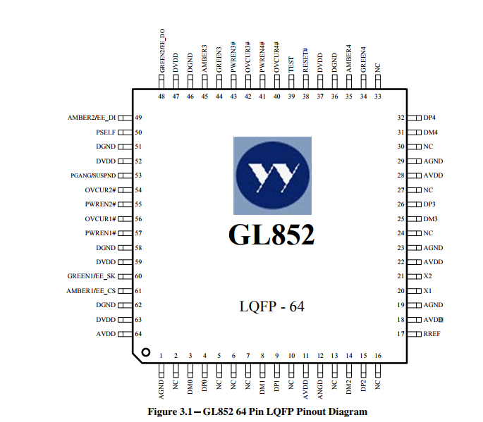
3.1 Pinouts
GL852
LQFP - 64
PWREN1# 57
DGND 58
DVDD 59
GREEN1/EE_SK 60
AMBER1/EE_CS 61
DGND 62
DVDD 63
AVDD 64
AMBER2/EE_DI 49
PSELF 50
DGND 51
DVDD 52
PGANG/SUSPND 53
OVCUR2# 54
PWREN2# 55
OVCUR1# 56 25

创维
LQFP64
USB
可长期供应