H5TQ2G63DFR/HYNIX/BGA/pdf规格书
地区:广东 深圳
认证:
无
图文详情
产品属性
相关推荐
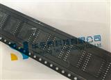
H5TQ2G63DFR图片


H5TQ2G63DFRDescription
While all addresses and
control inputs are latched on the rising edges of the CK (falling edges of the CK), Data, Data strobes and
Write data masks inputs are sampled on both rising and falling edges of it. The data paths are internally
pipelined and 8-bit prefetched to achieve very high bandwidth.
H5TQ2G63DFRFEATURES
• This product in compliance with the RoHS directive.
• VDD=VDDQ=1.5V +/- 0.075V
• Fully differential clock inputs (CK, CK) operation
• Differential Data Strobe (DQS, DQS)
• On chip DLL align DQ, DQS and DQS transition with CK
transition
• DM masks write data-in at the both rising and falling
edges of the data strobe
• All addresses and control inputs except data,
data strobes and data masks latched on the
rising edges of the clock
• Programmable CAS latency 5, 6, 7, 8, 9, 10, 11, 12, 13
and 14 supported
• Programmable additive latency 0, CL-1, and CL-2
supported
• Programmable CAS Write latency (CWL) = 5, 6, 7, 8
• Programmable burst length 4/8 with both nibble
sequential and interleave mode
• BL switch on the fly
• 8banks
• Average Refresh Cycle (Tcase 0 oC~ 95 oC)
- 7.8 μs at 0oC ~ 85 oC
- 3.9 μs at 85oC ~ 95 oC
Commercial Temperature( 0oC ~ 85 oC)
Industrial Temperature( -40oC ~ 95 oC)
• Auto Self Refresh supported
• JEDEC standard 78ball FBGA(x8), 96ball FBGA(x16)
• Driver strength selected by EMRS
• Dynamic On Die Termination supported
• Asynchronous RESET pin supported
• ZQ calibration supported
• TDQS (Termination Data Strobe) supported (x8 only)
• Write Levelization supported
• 8 bit pre-fetch
IDD and IDDQ Specification Parameters and Test Conditions
IDD and IDDQ Measurement Conditions
In this chapter, IDD and IDDQ measurement conditions such as test load and patterns are defined. Figure
1. shows the setup and test load for IDD and IDDQ measurements.
• IDD currents (such as IDD0, IDD1, IDD2N, IDD2NT, IDD2P0, IDD2P1, IDD2Q, IDD3N, IDD3P, IDD4R,
IDD4W, IDD5B, IDD6, IDD6ET, IDD6TC and IDD7) are measured as time-averaged currents with all
VDD balls of the DDR3 SDRAM under test tied together. Any IDDQ current is not included in IDD cur-
rents.
• IDDQ currents (such as IDDQ2NT and IDDQ4R) are measured as time-averaged currents with all
VDDQ balls of the DDR3 SDRAM under test tied together. Any IDD current is not included in IDDQ cur-
rents.
Attention: IDDQ values cannot be directly used to calculate IO power of the DDR3 SDRAM. They can
be used to support correlation of simulated IO power to actual IO power as outlined in Figure 2. In
DRAM module application, IDDQ cannot be measured separately since VDD and VDDQ are using one
merged-power layer in Module PCB.
For IDD and IDDQ measurements, the following definitions apply:
• ”0” and “LOW” is defined as VIN <= V ILAC(max).
• ”1” and “HIGH” is defined as VIN >= V IHAC(max).
• “MID_LEVEL” is defined as inputs are VREF = VDD/2.
• Timing used for IDD and IDDQ Measurement-Loop Patterns are provided in Table 1.
• Basic IDD and IDDQ Measurement Conditions are described in Table 2.
• Detailed IDD and IDDQ Measurement-Loop Patterns are described in Table 3 through Table 10.
• IDD Measurements are done after properly initializing the DDR3 SDRAM. This includes but is not lim-
ited to setting
RON = RZQ/7 (34 Ohm in MR1);
Qoff = 0 B (Output Buffer enabled in MR1);
RTT_Nom = RZQ/6 (40 Ohm in MR1);
RTT_Wr = RZQ/2 (120 Ohm in MR2);
TDQS Feature disabled in MR1
• Attention: The IDD and IDDQ Measurement-Loop Patterns need to be executed at least one time
before actual IDD or IDDQ measurement is started.
• Define D = {CS, RAS, CAS, WE}:= {HIGH, LOW, LOW, LOW}
• Define D = {CS, RAS, CAS, WE}:= {HIGH, HIGH, HIGH, HIGH}
H5TQ2G63DFR描述
尽管所有地址和控制输入的边缘上升的CK(CK)的边缘下降,数据,数据用闪光灯和面具写入数据输入采样在上升和下降的边缘。数据路径内部流水线和8位预取的实现非常高的带宽。
H5TQ2G63DFR特性
•VDD = VDDQ = 1.5 v + / - 0.075 v
•完全微分时钟输入(CK、CK)操作
•微分数据(dq,dq)
•在芯片DLL对齐DQ、DQ和DQ与CK过渡转型
•DM面具写数据输入的数据选通脉冲的上升和下降的边缘
•所有地址和控制输入,除了数据,数据用闪光灯和数据掩盖了锁定在时钟的上升的边缘
•可编程CAS延迟5、6、7、8、9、10、11、12、13和14支持
•可编程添加剂延迟0、CL-1 CL-2支持
•可编程脉冲时间4/8咬顺序和交错模式
•提单开关
•平均刷新周期(Tcase 0摄氏度~ 95摄氏度)
- μs at - 7.8 0oC ~ 85 oC
- 3.9μs在85度~ 95度
商业温度(0摄氏度~ 85摄氏度)
工业温度(-40度~ 95度)
•汽车自我更新的支持
•JEDEC标准78球FBGA(x8 -),96球FBGA(x16)
•驱动力量选择电子病历
•动态模终止支持
•异步复位销支持
•ZQ校准支持
•TDQS(终止数据选通)支持(×8只)
•写Levelization支持
•8位预取
IDD和IDDQ规范参数
IDD和IDDQ测试条件和测试条件
•IDD电流(例如IDD0、IDD1 IDD2N,IDD2NT,IDD2P0,IDD2P1,IDD2Q,IDD3N,IDD3P,IDD4R,IDD4W,IDD5B,IDD6,IDD6ET,IDD6TC和IDD7)测量是时间上的电流与所有VDD球DDR3 SDRAM测试下绑在一起。不包括任何IDDQ当前IDD。
•IDDQ电流(例如IDDQ2NT和IDDQ4R)测量上的电流与所有VDDQ球DDR3 SDRAM测试下绑在一起。不包括任何IDD当前IDDQ坏蛋——租金。
注意:
IDDQ值不能直接用来计算IO DDR3 SDRAM的力量。他们可以用来支持相关的模拟输入输出功率实际输入输出功率如图2中列出。分别在DRAM模块应用程序中,IDDQ无法衡量自VDD VDDQ使用模块PCB merged-power层之一。
对于IDD和IDDQ测试,以下定义适用:
•“0”和“低”的定义是VIN < = V ILAC(max)。
•“1”和“高”被定义为VIN > = V IHAC(max)。
•“MID_LEVEL”被定义为输入VREF = VDD / 2。
•时间用于IDD和IDDQ Measurement-Loop模式是表1中提供。
•基本IDD和IDDQ测试条件如表2中所描述的。
•详细IDD和IDDQ Measurement-Loop模式是描述在表3表10。
•IDD测量正确初始化DDR3 SDRAM后完成。这包括但不仅lim -报道设置
•注意:IDD和IDDQ Measurement-Loop模式需要执行至少一个实际IDD或IDDQ测试开始时间。
•定义D = { CS,RAS,中科院,我们}:= {高、低、低、低}
•定义D = { CS,RAS,中科院,我们}:= {高,高,高,高}
H5TQ2G63DFR
HYNIX
BGA
2017+