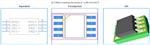
The MachXO family architecture contains an array of logic blocks surrounded by Programmable I/O (PIO). Some
devices in this family have sysCLOCK PLLs and blocks of sysMEM™ Embedded Block RAM (EBRs). Figures 2-1,
2-2, and 2-3 show the block diagrams of the various family members.
The logic blocks are arranged in a two-dimensional grid with rows and columns. The EBR blocks are arranged in a
column to the left of the logic array. The PIO cells are located at the periphery of the device, arranged into Banks.
The PIOs utilize a flexible I/O buffer referred to as a sysIO interface that supports operation with a variety of interface standards. The blocks are connected with many vertical and horizontal routing channel resources. The place
and route software tool automatically allocates these routing resources.
There are two kinds of logic blocks, the Programmable Functional Unit (PFU) and the Programmable Functional
unit without RAM (PFF). The PFU contains the building blocks for logic, arithmetic, RAM, ROM, and register functions. The PFF block contains building blocks for logic, arithmetic, ROM, and register functions. Both the PFU and
PFF blocks are optimized for flexibility, allowing complex designs to be implemented quickly and effectively. Logic
blocks are arranged in a two-dimensional array. Only one type of block is used per row.