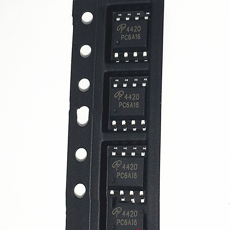


AO4420 液晶高压板MOS管 全新现货热
地区:广东 深圳
认证:
无
图文详情
产品属性
相关推荐

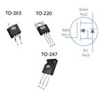
N-Channel 30-V (D-S) MOSFET
VDS (V) ID(A)
13.8
13.2
Symbol Limit Units
VDS 30
VGS ±20
TA=25°C 13.8
TA=70°C 11.6
IDM 50
IS 4.6 A
TA=25°C 3.1
TA=70°C 2.2
TJ
, Tstg -55 to 150 °C
Symbol Maximum Units
40
80
Notes
a. Surface Mounted on 1” x 1” FR4 Board.
b. Pulse width limited by maximum junction temperature
Pulsed Drain Current b
Continuous Source Current (Diode Conduction) a
THERMAL RESISTANCE RATINGS
°C/W
Parameter
Operating Junction and Storage Temperature Range
ABSOLUTE MAXIMUM RATINGS (TA = 25°C UNLESS OTHERWISE NOTED)
V
Parameter
Drain-Source Voltage
Maximum Junction-to-Ambient a
Continuous Drain Current a
PRODUCT SUMMARY
30
rDS(on) (mΩ)
11 @ VGS = 4.5V
12 @ VGS = 2.5V
Gate-Source Voltage
Power Dissipation a
t <= 10 sec
Steady State
RθJA
ID
A
PD W
Key Features:
• Low rDS(on) trench technology
• Low thermal impedance
• Fast switching speed
Typical Applications:
• White LED boost converters
• Automotive Systems
• Industrial DC/DC Conversion Circuits
AO4420
美国万代AOS
SOP-8
无铅环保型
贴片式
盒带编带包装
中功率
中国
全新原装