图文详情
产品属性
相关推荐
Device Overview
Summary
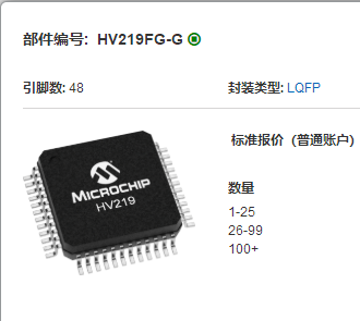
HV219 is a low switch resistance, low charge injection, 8-channel, 200V, analog switch integrated circuit (IC) intended primarily for medical ultrasound imaging. The device can also be used for NDE (non-destructive evaluation) applications. The HV219 is a lower switch resistance, 11O versus 22O, version of HV20220 device. The lower switch resistance will help reduce insertion loss. It has the same pin configuration as that of HV20220PJ and the HV20220FG. The device is manufactured using HVCMOS (high voltage CMOS) technology with high voltage bilateral DMOS structures for the outputs and low voltage CMOS logic for the input control. The outputs are configured as eight independent single pole single throw 11O analog switches. The input logic is an 8-bit serial to parallel shift register followed by an 8-bit parallel latch. The switch states are determined by the data in the latch. Logic high will correspond to a closed switch and logic low as an opened switch. The HV219 is designed to operate on various combinations of high voltage supplies. For example the VPP and VNN supplies can be: +40V/-160V, +100V/-100V, or +160V/-40V. This allows the user to maximize the signal voltage for uni-polar negative, bi-polar, or uni-polar positive.
Additional Features
HVCMOS technology for high performance
Very low quiescent power dissipation (-10μA)
Output on-resistance typically 11Ω
Low parasitic capacitance
DC to 50MHz small signal frequency response
-60dB typical off-isolation at 5.0MHz
CMOS logic circuitry for low power
Excellent noise immunity
Serial shift register logic control with latches
Flexible operating supply voltages
Surface mount packages
Features:
HVCMOS technology for high performance
Very low quiescent power dissipation (-10μA)
Output on-resistance typically 11Ω
Low parasitic capacitance
DC to 50MHz small signal frequency response
-60dB typical off-isolation at 5.0MHz

MICROCHIP
QFP
6000
面议
2000