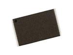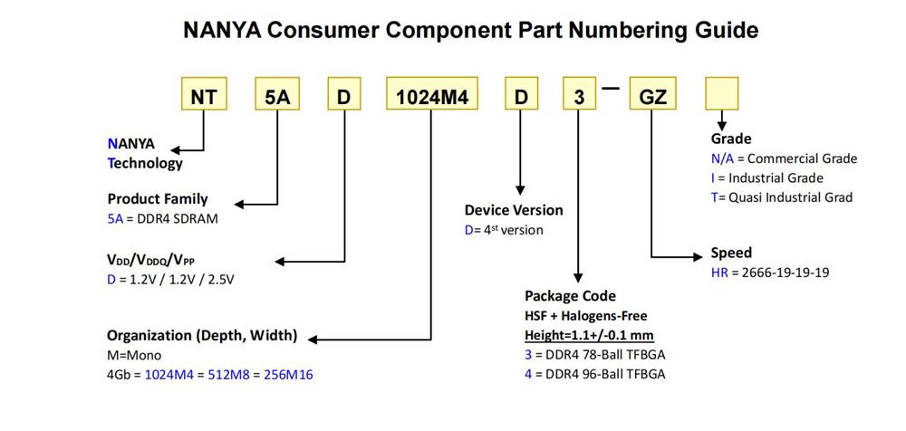


原装NT5AD256M16D4-HR DRAM DDR4
地区:广东 深圳
认证:
无
图文详情
产品属性
相关推荐
原装NT5AD256M16D4-HR DRAM DDR4
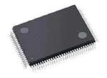
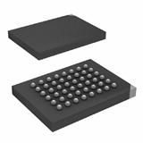
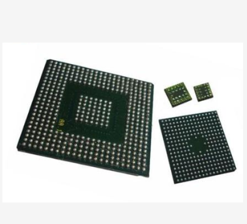
NT5AD256M16D4-HR DRAM DRAM Chip DDR4 SDRAM 4Gbit 256Mx16 1.2V 96-Pin TFBGA
Commercial and Industrial DDR4 4Gb SDRAM
NT5AD256M16D4-HR DRAM的技术参数:
制造商 : 南亚
存储器组织 : 256MX16
速度 : 1333MHZ
无铅/环保 : 无铅/环保
封装 : BGA
存储器类型 : DDR4 SDRAM
容量 : 4Gb
NT5AD256M16D4-HR DRAM的基本功能
he DDR4 SDRAM is a high-speed dynamic random-access memory internally configured as sixteen-banks, 4 bank group with 4 banks for each bank group for x8 and eight-banks, 2 bank group with 4 banks for each bank group for x16 DRAM. The DDR4 SDRAM uses a 8n prefetch architecture to achieve high-speed operation. The 8n prefetch architecture is combined with an interface designed to transfer two data words per clock cycle at the I/O pins.
A single read or write operation for the DDR4 SDRAM consists of a single 8n-bit wide, four clock data transfer at the internal DRAM core and eight corresponding n-bit wide, one-half clock cycle data transfers at the I/O pins.
Read and write operation to the DDR4 SDRAM are burst oriented, start at a selected location, and continue for a burst length of eight or a ‘chopped’ burst of four in a programmed sequence.
Operation begins with the registration of an ACTIVATE Command, which is then followed by a Read or Write command. The address bits registered coincident with the ACTIVATE Command are used to select the bank and row to be activated (BG0-BG1 in x8 and BG0 in x16 select the bank group; BA0-BA1 select the bank; A0-A15 select the row; refer to Addressing section for more details.
The address bits registered coincident with the Read or Write command are used to select the starting column location for the burst operation, determine if the auto precharge command is to be issued (via A10), and select BC4 or BL8 mode ‘on the fly’ (via A12) if enabled in the mode register.


NT5AD256M16D4-HR
NANYA/南亚
BGA
21+
4GB